Dc electrical characteristics (continued), Ac electrical characteristics – Rainbow Electronics MAX7311 User Manual
Page 3
MAX7311
2-Wire-Interfaced 16-Bit I/O Port Expander
with Interrupt
_______________________________________________________________________________________
3
Note 1: All parameters are 100% production tested at T
A
= +25°C. Specifications over temperature are guaranteed by design.
Note 2: Minimum SCL clock frequency is limited by the MAX7311 bus timeout feature, which resets the serial bus interface if either
SDA or SCL is held low for a minimum of 25ms. Disable bus timeout feature for DC operation.
Note 3: A master device must internally provide a hold time of at least 300ns for the SDA signal (referred to the V
IL
of the SCL
signal) in order to bridge the undefined region SCL’s falling edge.
Note 4: C
B
= total capacitance of one bus line in pF.
Note 5: The maximum t
F
for the SDA and SCL bus lines is specified at 300ns. The maximum fall time for the SDA output stage t
F
is
specified at 250ns. This allows series protection resistors to be connected between the SDA and SCL pins and the
SDA/SCL bus lines without exceeding the maximum specified t
F
.
Note 6: Input filters on the SDA and SCL inputs suppress noise spikes less than 50ns.
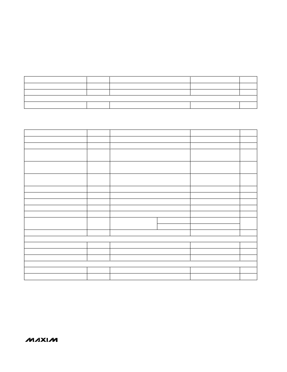
DC ELECTRICAL CHARACTERISTICS (continued)
(V+ = 2V to 5.5V, T
A
= -40°C to +125°C, unless otherwise noted. Typical values are at V+ = 3.3V, T
A
= +25°C.) (Note 1)
PARAMETER
SYM B O L CONDITIONS
MIN
TYP
MAX
UNITS
Leakage Current
-1
+1
µA
Input Capacitance
4
pF
INT
Low-Level Output Current
I
OL
V
OL
= 0.4V
6
mA
AC ELECTRICAL CHARACTERISTICS
(V+ = 2V to 5.5V, T
A
= -40°C to +125°C, unless otherwise noted.) (Note 1)
PARAMETER
SYM B O L CONDITIONS
MIN
TYP
MAX
UNITS
SCL Clock Frequency
f
SCL
(Note 2)
400
kHz
Bus Timeout
t
TIMEOUT
29
61
ms
Bus Free Time Between STOP
and START Conditions
t
BUF
Figure 2
1.3
µs
Hold Time (Repeated) START
Condition
t
HD,STA
Figure 2
0.6
µs
Repeated START Condition
Setup Time
t
SU,STA
Figure 2
0.6
µs
STOP Condition Setup Time
t
SU,STO
Figure 2
0.6
µs
Data Hold Time
t
HD,DAT
Figure 2 (Note 3)
0.9
µs
Data Setup Time
t
SU,DAT
Figure 2
100
ns
SCL Low Period
t
LOW
Figure 2
1.3
µs
SCL High Period
t
HIGH
Figure 2
0.7
µs
V+ < 3.3V
500
SDA Fall Time
t
F
Figure 2 (Notes 4, 5)
V+
≥ 3.3V
250
ns
Pulse Width of Spike Suppressed
t
SP
(Note 6)
50
ns
PORT TIMING
Output Data Valid
t
PV
Figure 7
3
µs
Input Data Setup Time
27
µs
Input Data Hold Time
0
µs
INTERRUPT TIMING
Interrupt Valid
t
IV
Figure 9
30.5
µs
Interrupt Reset
t
IR
Figure 9
2
µs