Applications information, Table 6. register 0x08—timeout register – Rainbow Electronics MAX7311 User Manual
Page 11
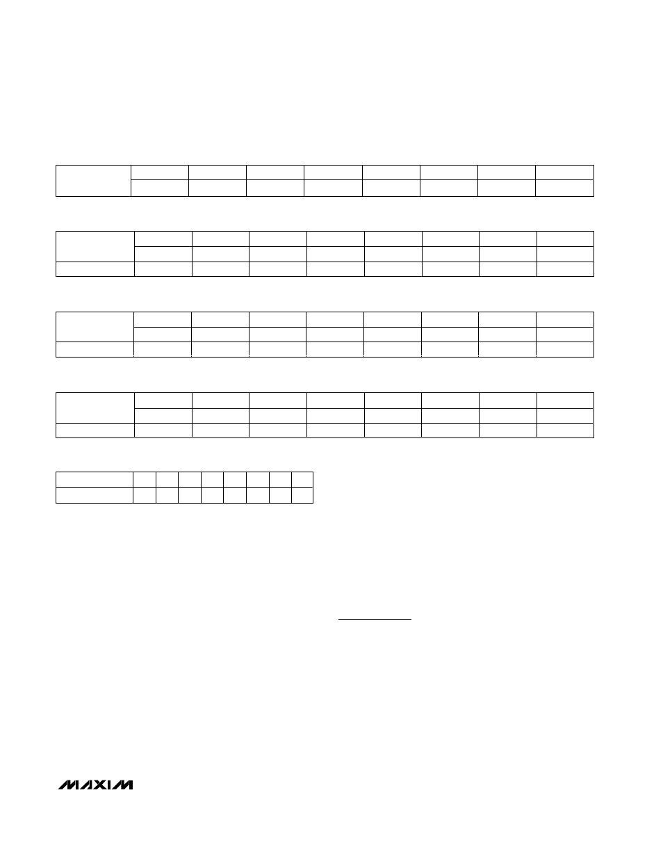
Output Port Registers
The output port registers (Table 3) set the outgoing
logic levels of the I/Os defined as outputs by the
respective configuration register. Reads from the out-
put port registers reflect the value that is in the flip-flop
controlling the output selection, not the actual I/O value.
Polarity Inversion Registers
The polarity inversion registers (Table 4) enable polarity
inversion of pins defined as inputs by the respective
port configuration registers. Set the bit in the polarity
inversion register to invert the corresponding port pin’s
polarity. Clear the bit in the polarity inversion register to
retain the corresponding port pin’s original polarity.
Configuration Registers
The configuration registers (Table 5) configure the
directions of the I/O pins. Set the bit in the respective
configuration register to enable the corresponding port
as an input. Clear the bit in the configuration register to
enable the corresponding port as an output.
Bus Timeout
Set register 0x08 LSB (bit 0) to enable the bus timeout
function (Table 6) or clear it to disable the bus timeout
function. Enabling the timeout feature resets the
MAX7311 serial bus interface when SCL stops either high
or low during a read or write. If either SCL or SDA is low
for more than 29ms after the start of a valid serial transfer,
the interface resets itself and sets up SDA as an input.
The MAX7311 then waits for another START condition.
Standby
The MAX7311 goes into standby when the I
2
C bus is
idle. Standby supply current is typically 2.9µA.
Applications Information
Power-Supply Consideration
The MAX7311 operates from a supply voltage of 2V to
5.5V. Bypass the power supply to GND with a 0.047µF
capacitor as close to the device as possible.
MAX7311
2-Wire-Interfaced 16-Bit I/O Port Expander
with Interrupt
______________________________________________________________________________________
11
I7
I6
I5
I4
I3
I2
I1
I0
BIT
I15
I14
I13
I12
I11
I10
I9
I8
Table 2. Registers 0x00, 0x01—Input Port Registers
O7
O6
O5
O4
O3
O2
O1
O0
BIT
O15
O14
O13
O12
O11
O10
O9
O8
Power-up default
1
1
1
1
1
1
1
1
Table 3. Registers 0x02, 0x03—Output Port Registers
I/O7
I/O6
I/O5
I/O4
I/O3
I/O2
I/O1
I/O0
BIT
I/O15
I/O14
I/O13
I/O12
I/O11
I/O10
I/O9
I/O8
Power-up default
0
0
0
0
0
0
0
0
Table 4. Registers 0x04, 0x05—Polarity Inversion Registers
I/O7
I/O6
I/O5
I/O4
I/O3
I/O2
I/O1
I/O0
BIT
I/O15
I/O14
I/O13
I/O12
I/O11
I/O10
I/O9
I/O8
Power-up default
1
1
1
1
1
1
1
1
Table 5. Registers 0x06, 0x07—Configuration Registers
BIT
7
6
5
4
3
2
1
0
Power-up default
0
0
0
0
0
0
0
1
Table 6. Register 0x08—Timeout Register