Rainbow Electronics MAX7311 User Manual
Page 2
MAX7311
2-Wire-Interfaced 16-Bit I/O Port Expander
with Interrupt
2
_______________________________________________________________________________________
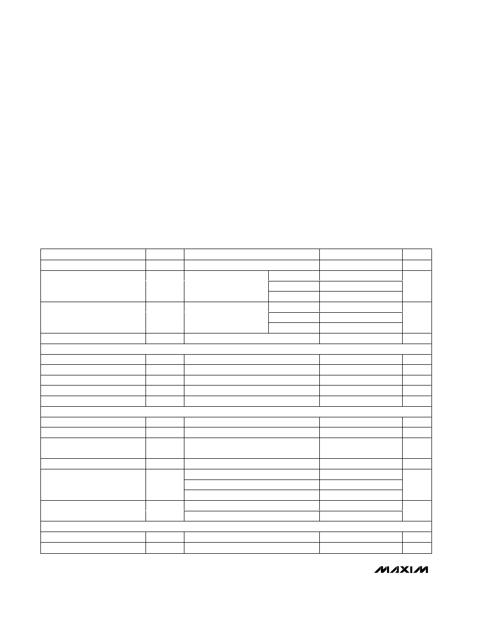
ABSOLUTE MAXIMUM RATINGS
DC ELECTRICAL CHARACTERISTICS
(V+ = 2V to 5.5V, T
A
= -40°C to +125°C, unless otherwise noted. Typical values are at V+ = 3.3V, T
A
= +25°C.) (Note 1)
Stresses beyond those listed under “Absolute Maximum Ratings” may cause permanent damage to the device. These are stress ratings only, and functional
operation of the device at these or any other conditions beyond those indicated in the operational sections of the specifications is not implied. Exposure to
absolute maximum rating conditions for extended periods may affect device reliability.
V
+
to GND ................................................................-0.3V to +6V
I/O0–I/O15 as Inputs ....................................(GND - 0.3V) to +6V
SCL, SDA, AD0, AD1, AD2, INT...................(GND - 0.3V) to +6V
Maximum V
+
Current ......................................................+250mA
Maximum GND Current ...................................................-250mA
DC Input Current on I/O0–I/O15 .......................................±20mA
DC Output Current on I/O0–I/O15 ....................................±80mA
Continuous Power Dissipation (T
A
= +70°C)
24-Pin Wide SO (derate 11.8mW/°C above +70°C) ....941mW
24-Pin SSOP (derate 8.0mW/°C above +70°C) ...........640mW
24-Pin TSSOP (derate 12.2mW/°C above +70°C) .......975mW
24-Pin Thin QFN (derate 20.8mW/°C above +70°C) .1668mW
Operating Temperature Range .........................-40°C to +125°C
Junction Temperature ......................................................+150°C
Storage Temperature Range .............................-65°C to +150°C
Lead Temperature (soldering, 10s) .................................+300°C
PARAMETER
SYM B O L CONDITIONS
MIN
TYP
MAX
UNITS
Supply Voltage
V
+
2
5.5
V
V
+
= 2V
23
35
V
+
= 3.3V
43
60
Supply Current
I
+
All I/Os unloaded,
f
SCL
= 400kHz
V
+
= 5.5V
80
120
µA
V
+
= 2V
2.3
11
V
+
= 3.3V
2.9
12
Standby Current
I
STBY
All I/Os unloaded,
f
SCL
= 0
V
+
= 5.5V
3.8
15.5
µA
Power-On Reset Voltage
V
POR
1.4
1.7
V
SCL, SDA
Input Voltage Low
V
IL
0.3
✕
V
+
V
Input Voltage High
V
IH
0.7
✕
V
+
V
Low-Level Output Voltage
V
OL
I
SINK
= 6mA
0.4
V
Leakage Current
I
L
-1
+1
µA
Input Capacitance
10
pF
I/O_
Input Voltage Low
V
IL
0.8
V
Input Voltage High
V
IH
1.8
V
Input Leakage Current
T
A
= -40°C to +85°C; includes internal
pullup current, V
IO
= V
+
1
µA
Internal Pullup Current
T
A
= -40°C to +85°C, V
IO
= 0
34
100
µA
V
+
= 2V, V
OL
= 0.5V
8.5
17
V
+
= 3.3V, V
OL
= 0.5V
17
32
Low-Level Output Current
I
SINK
V
+
= 5V, V
OL
= 0.5V
43
mA
V
+
= 3.3V, V
OH
= 2.4V
29
41
High Output Current
I
SOURCE
V
+
= 5V, V
OH
= 4.5V
31
mA
AD0, AD1, AD2
Input Voltage Low
V
IL
0.3
✕
V
+
V
Input Voltage High
V
IH
0.7
✕
V
+
V