Rainbow Electronics MAXQ7667 User Manual
Page 26
MAXQ7667
16-Bit, RISC, Microcontroller-Based,
Ultrasonic Distance-Measuring System
26
______________________________________________________________________________________
Connect bypass capacitors at each power-supply input
as close as possible to the device. Use a bypass
capacitor less than 0.47µF on DVDDIO. For most appli-
cations, 0.1µF bypass capacitors are adequate.
Supply Brownout Monitor
Power supplies DVDD, AVDD, and DVDDIO each
include a brownout monitor/supervisor that alerts the
µC when their corresponding supply voltages drop
below the interrupt threshold. Activate each brownout
monitor independently using the corresponding
brownout enable bits: VDBE, VIBE, and VABE.
Reset
In reset mode, no instruction execution occurs and all
inputs/outputs return to their default states. Code exe-
cution resumes at address 8000h (in the utility ROM)
once the reset condition is removed.
Four different sources reset the MAXQ7667: POR,
watchdog timer reset, external reset, and internal sys-
tem reset.
During normal operation, force
RESET low for at least
four system clock cycles for an external reset. Set the
ROD bit in the SC register, while the SPE bit in the ICDF
register is set, for an internal system reset. See Section
16 of the
MAXQ7667 User’s Guide
.
Power-On Reset (POR)
The MAXQ7667 includes a DVDD voltage supervisor to
control the µC POR. On power-up, internal circuitry
pulls
RESET low and resets all the internal registers.
RESET is held low for the duration of the power-on
delay after V
DVDD
rises above the DVDD reset thresh-
old. The internal RC oscillator starts up and software
execution begins at the reset vector location 8000h
immediately after the device exits POR while
RESET is
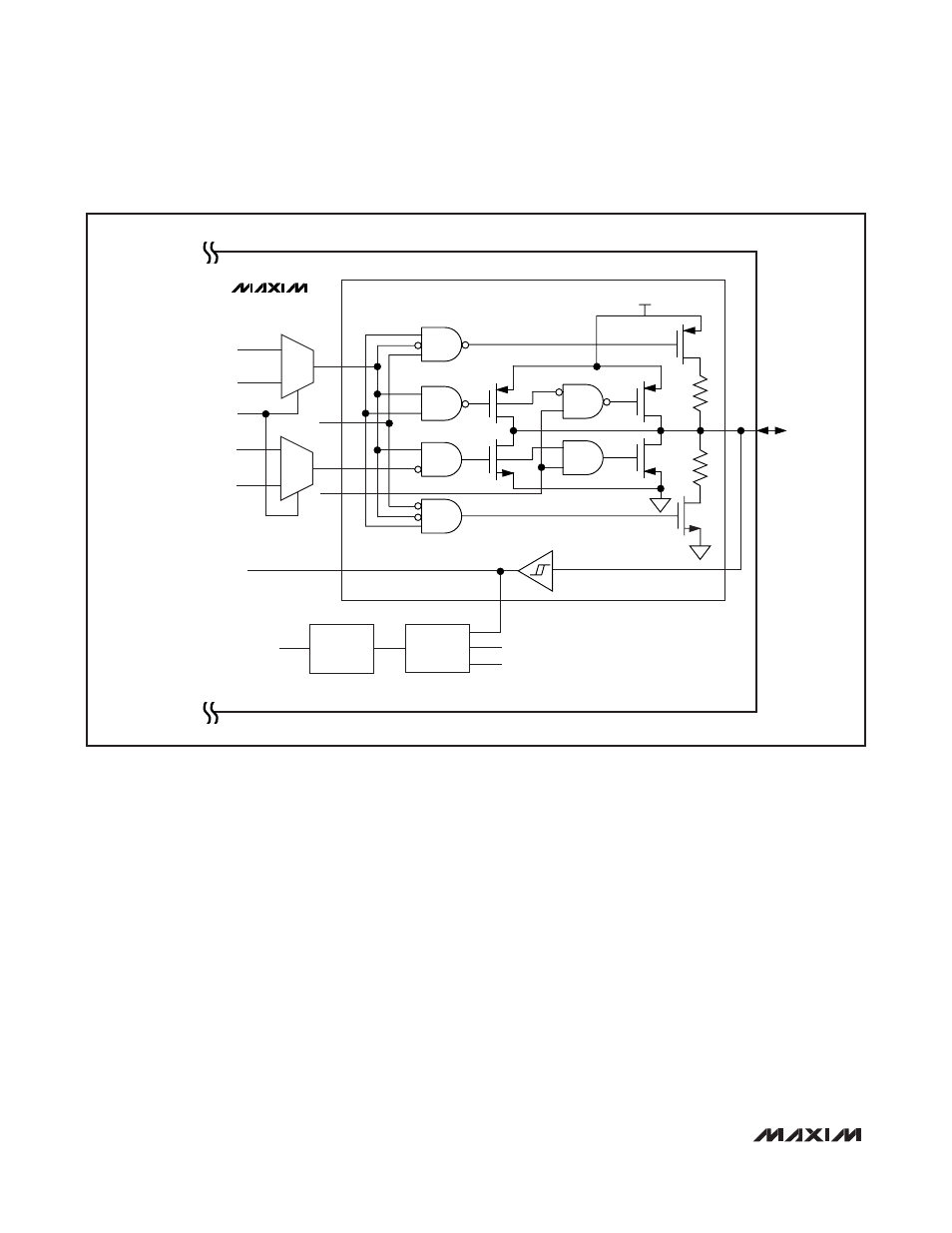
I/O PAD
DVDDIO
P0._
100
ΩK
100
ΩK
DGND
DGND
EIE0._
EIES0._
DETECT
CIRCUIT
INTERRUPT
FLAG
PS0._
PR0._
PD0._
PO0._
SF DIRECTION
SF ENABLE
SF OUTPUT
PI0._ OR
SF INPUT
FLAG
MUX
MUX
MAXQ7667
Figure 13. Port 0 Digital I/O Basic Circuitry. Port 1 Circuitry is the Same as Port 2.