Sar adc, Digital comparator and threshold adjust – Rainbow Electronics MAXQ7667 User Manual
Page 19
MAXQ7667
16-Bit, RISC, Microcontroller-Based,
Ultrasonic Distance-Measuring System
______________________________________________________________________________________
19
output to the FIFO automatically each time the lowpass
filter output updates, through the control of one of the
timer outputs, or through software. The device includes
a FIFO depth counter with programmable interrupt lev-
els and generates an interrupt if a FIFO overflow condi-
tion occurs. The output of the digital lowpass filter
connects to a digital comparator that can generate an
interrupt for a specified echo signal level.
Digital Comparator and Threshold Adjust
The digital comparator output asserts when the echo
amplitude at the output of the digital lowpass filter cross-
es a given threshold. The comparator’s threshold level,
hysteresis, and interrupt polarity are programmable.
SAR ADC
The MAXQ7667 incorporates a 12-bit unbuffered SAR
ADC with sample-and-hold and conversion rate up to
250ksps. The ADC allows measurements of tempera-
ture, battery voltage, or other parameters using five sin-
gle-ended or two fully differential analog inputs
(AIN0–AIN4). All of the analog inputs have a range of 0
to V
REF
in unipolar mode and ±V
REF
/2 in bipolar mode.
The SAR ADC supports three different conversion start
sources: timers, ADC control input (ADCCTL), and soft-
ware write. The conversion start source triggers the
ADC acquisition and conversion. The system clock pro-
vides the ADC clock frequency programmable to 1/2,
1/4, 1/8, or 1/16 of the system clock. Use internal
bandgap reference, external reference, or AVDD for
voltage reference of the SAR ADC. Figure 3 shows a
simplified block diagram of the SAR ADC.
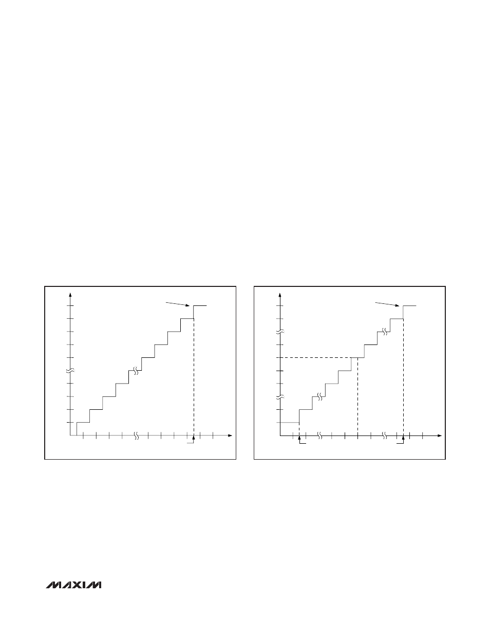
The output of the SAR ADC is straight binary in unipolar
mode and two’s complement in bipolar mode. Figures 4
and 5 show the ADC transfer functions in unipolar
mode and bipolar mode.
000
001
002
003
004
FFC
FFB
FFD
FFE
FFF
0
1
2
3
4
FS
FS - 1.5 LSB
FULL-SCALE
TRANSITION
FS = REF
ZS = 0
1 LSB = REF/4096
OUTPUT CODE (hex)
DIFFERENTIAL INPUT VOLTAGE (LSB)
Figure 4. Unipolar Transfer Function
800
801
FFE
001
000
FFF
7FE
7FF
-FS
0
+FS
OUTPUT CODE (hex)
DIFFERENTIAL INPUT VOLTAGE (LSB)
+FS - 1.5 LSB
FULL-SCALE
TRANSITION
+FS = REF/2
ZS = 0
-FS = -REF/2
1 LSB = REF/4096
-FS + 0.5 LSB
Figure 5. Bipolar Transfer Function