Rainbow Electronics MAXQ7667 User Manual
Page 2
MAXQ7667
16-Bit, RISC, Microcontroller-Based,
Ultrasonic Distance-Measuring System
2
_______________________________________________________________________________________
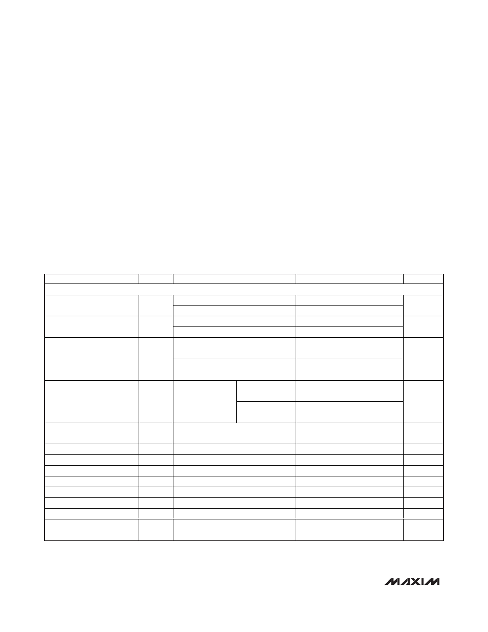
ABSOLUTE MAXIMUM RATINGS
ELECTRICAL CHARACTERISTICS
(V
DVDDIO
= +5V, V
AVDD
= +3.3V; V
DVDD
= +2.5V, system clock (f
SYSCLK
) = 16MHz, burst frequency (f
BURST
) = bandpass frequency
(f
BPF
) = 50kHz, C
REFBG
= C
REF
= 1µF in parallel with 0.01µF, f
ADCCLK
= 2MHz (SAR data rate = 125ksps), T
A
= T
MIN
to T
MAX
, unless
otherwise specified. Typical values are at T
A
= +25°C.)
Stresses beyond those listed under “Absolute Maximum Ratings” may cause permanent damage to the device. These are stress ratings only, and functional
operation of the device at these or any other conditions beyond those indicated in the operational sections of the specifications is not implied. Exposure to
absolute maximum rating conditions for extended periods may affect device reliability.
DVDDIO, GATE5, REG3P3, REG2P5 to
DGND ................................................................-0.3V to +6.0V
AVDD to AGND .....................................................-0.3V to +4.0V
DVDD to DGND .....................................................-0.3V to +3.0V
DVDDIO to DVDD..................................................-0.3V to +6.0V
AVDD to DVDD......................................................-0.3V to +4.0V
AGND to DGND.....................................................-0.3V to +0.3V
Digital Inputs/Outputs to DGND..........-0.3V to (V
DVDDIO
+ 0.3V)
Analog Inputs/Outputs to AGND ............-0.3V to (V
AVDD
+ 0.3V)
XIN, XOUT to DGND ..............................-0.3V to (V
DVDD
+ 0.3V)
Maximum Current into Any Pin............................................50mA
Continuous Power Dissipation (T
A
= +70°C)
48-Pin LQFP (derate 21.7mW/°C above +70°C).....1739.1mW
Operating Temperature Range .........................-40°C to +125°C
Storage Temperature Range .............................-60°C to +150°C
Lead Temperature (soldering, 10s) .................................+300°C
PARAMETER
SYMBOL
CONDITIONS
MIN
TYP
MAX
UNITS
ECHO INPUT (Low-Noise Amplifier and Sigma-Delta ADC)
VGA gain adjust = 1.55µV
P-P
/LSB
5.6
Input-Referred Noise
(Note 1)
VGA gain adjust = 0.1µV
P-P
/LSB
0.7
µV
RMS
VGA gain adjust = 1.55µV
P-P
/LSB 80
Minimum Detectable Signal
VGA gain adjust = 0.1µV
P-P
/LSB
10
µV
P-P
VGA gain adjust = 1.55µV
P-P
/LSB,
unclipped
100
Operating Input Range
VGA gain adjust = 0.1µV
P-P
/LSB,
unclipped
6.7
mV
P-P
VGA gain adjust
= 1.55µV
P-P
/LSB
1.55
Programmable Gain
From echo input to
bandpass filter in
reply to input
VGA gain adjust
= 0.1µV
P-P
/LSB
0.1
µV
P-P
/LSB
Programmable-Gain Adjust
Resolution
(Note
2)
10
%
LNA Bandwidth
150
kHz
ADC Sampling Rate
80 x f
BPF
kHz
ADC Output Data Rate
10 x f
BPF
kHz
ADC Output Data Resolution
16
Bits
Echo-Input Resistance R
IN
For each echo input
14
k
Echo-Input Capacitance
14
pF
Echo-Input DC Bias Voltage
V
AVDD
/2
V
Maximum Overvoltage
Recovery Time
Recover
from
2V
P-P
input
10
µs