Pin description (continued) – Rainbow Electronics MAXQ7667 User Manual
Page 13
MAXQ7667
16-Bit, RISC, Microcontroller-Based,
Ultrasonic Distance-Measuring System
______________________________________________________________________________________
13
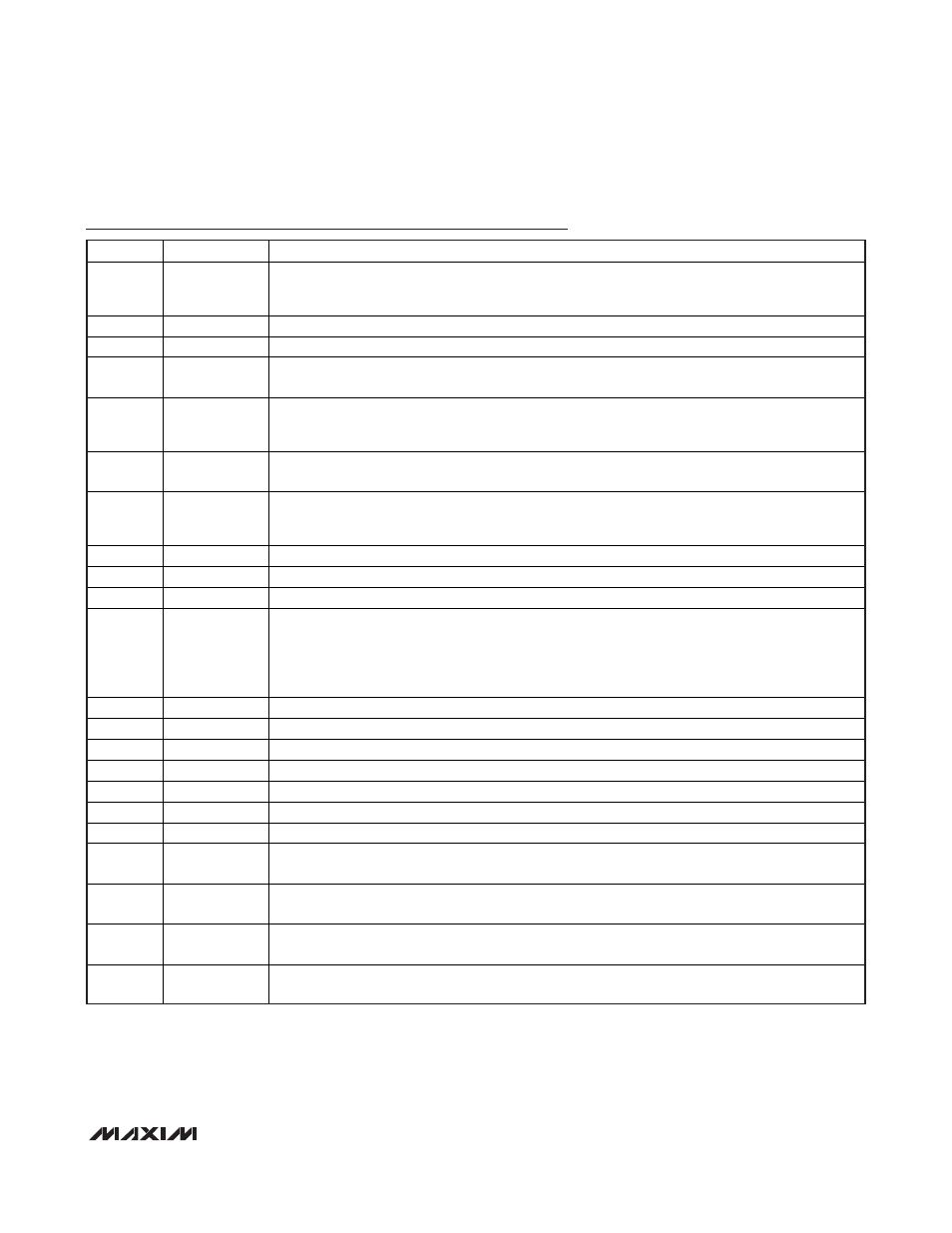
Pin Description (continued)
PIN
NAME
FUNCTION
21 XOUT
Crystal Oscillator Output. Connect an external crystal or resonator between XIN and XOUT. Leave
XOUT unconnected when driving XIN with a 2.5V level clock or when an external clock source is
not used.
22
REG2P5
+2.5V Voltage Regulator Output
23 REG3P3
+3.3V
Voltage
Regulator
Output
24 GATE5
+5V DVDDIO Voltage Regulator Control Output. GATE5 controls an external npn or nMOS
transistor that passes power to DVDDIO.
25
RESET
Reset Input/Output.
RESET is open drain with an internal pullup resistor to DVDDIO. Internal
circuitry pulls
RESET low when V
DVDDIO
falls below its brownout reset value or watchdog reset is
enabled and the watchdog timeout period expires. Force
RESET low externally for manual reset.
26 FILT
PLL VCO Control Input. Connect external filter components on FILT for the internal PLL circuit. See
the Typical Application Circuit/Functional Diagram.
27, 32
AVDD
Analog Supply Voltage. Connect all AVDD inputs directly to a +3.3V source or to REG3P3 for self-
powered operation. Bypass each AVDD to AGND with a 0.1µF capacitor as close as possible to
the device.
28, 31, 33
AGND
Analog Ground. Connect all AGND nodes together. Connect to DGND at a single point.
29
ECHON
Negative Echo Input. AC-couple ECHON to an ultrasonic transducer.
30
ECHOP
Positive Echo Input. AC-couple ECHOP to an ultrasonic transducer.
34 REF
ADC Reference Input/Reference Buffer Output. When using the internal reference, the buffered
bandgap reference voltage (V
REF
) is provided for both SAR and sigma-delta ADCs. When using an
external reference, apply an external voltage source ranging between 1V and V
AVDD
at REF.
Disable the reference buffer when applying an external reference at REF. Bypass REF to AGND
with a 0.47µF capacitor.
35
REFBG
+2.5V Reference Output/Reference Buffer Input. Bypass to AGND with a 0.47µF capacitor.
36
AIN0
SAR ADC Input 0. AIN0 pairs with AIN1 in differential mode.
37
AIN1
SAR ADC Input 1. AIN1 pairs with AIN0 in differential mode.
38
AIN2
SAR ADC Input 2. AIN2 pairs with AIN3 in differential mode.
49
AIN3
SAR ADC Input 3. AIN3 pairs with AIN2 in differential mode.
40
AIN4
SAR ADC Input 4
41
N.C.
No Connection. Internally connected. Leave unconnected.
45 BURST
Burst Output. Burst is the ultrasonic transducer excitation pulse output. BURST remains in three-
state mode on power-up.
46 P1.0/TDO
Port 1 Data 0/JTAG Output. P1.0 is a general-purpose digital I/O. TDO is the JTAG serial data
output. Refer to the MAXQ7667 User’s Guide Sections 5 and 11.
47 P1.1/TMS
Port 1 Data 1/JTAG Test Mode-Select Input. P1.1 is a general-purpose digital I/O. TMS is the JTAG
mode-select input. Refer to the MAXQ7667 User’s Guide Sections 5 and 11.
48 P1.2/TDI
Port 1 Data 2/JTAG Input. P1.2 is a general-purpose digital I/O. TDI is the JTAG serial data input.
Refer to the MAXQ7667 User’s Guide Sections 5 and 11.