Voltage reference, Schedule timer – Rainbow Electronics MAXQ7667 User Manual
Page 20
MAXQ7667
16-Bit, RISC, Microcontroller-Based,
Ultrasonic Distance-Measuring System
20
______________________________________________________________________________________
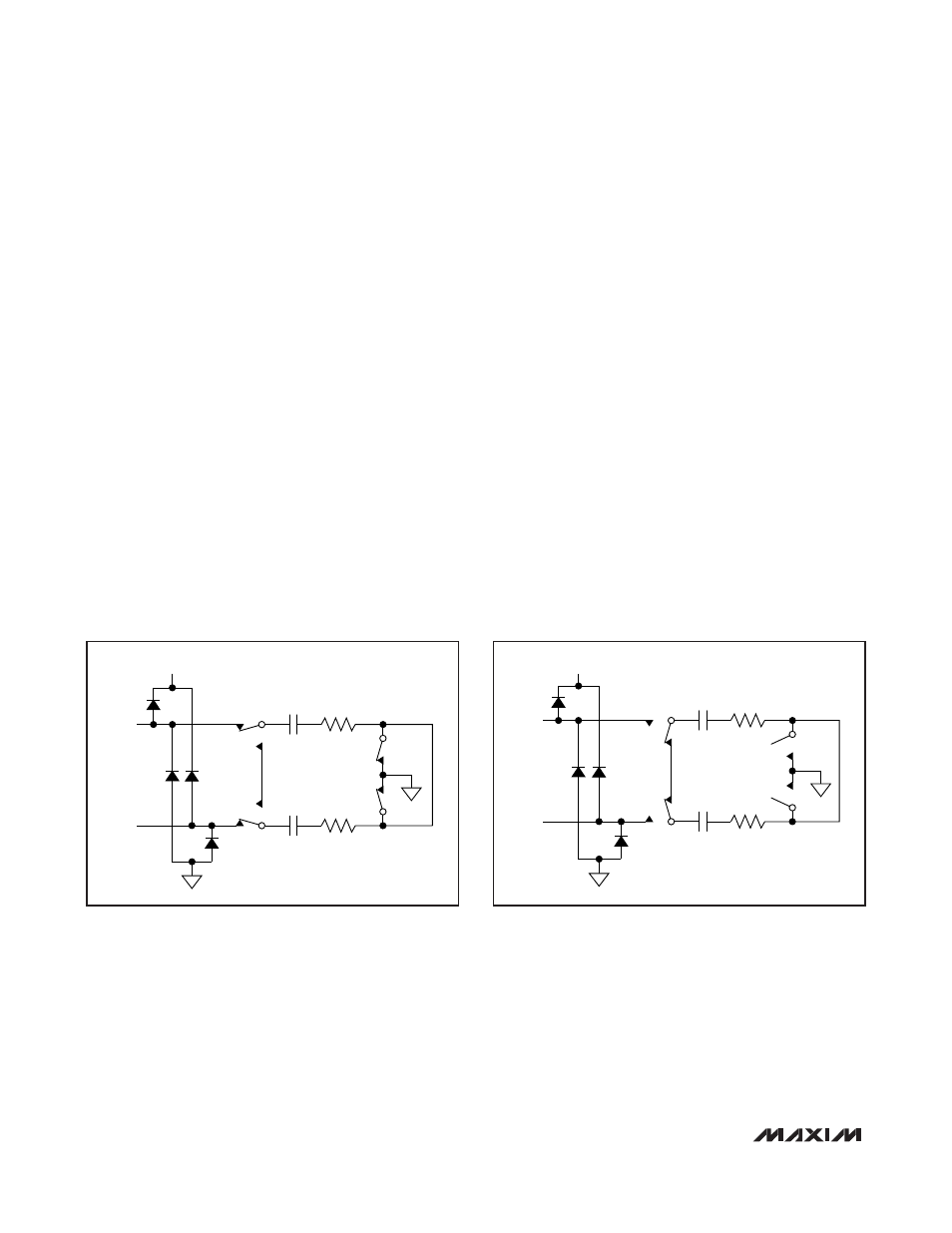
SAR ADC Analog Input Track-and-Hold (T/H)
Figures 6 and 7 show the equivalent input circuit of the
MAXQ7667 analog input architecture. During acquisi-
tion (track), a sampling capacitor charges to the posi-
tive input voltage at AIN0–AIN4 in single-ended mode
or AIN0 and AIN2 in differential mode while a second
sampling capacitor connects to AGND in single-ended
mode or AIN1 and AIN3 in differential mode. The ADC
conversion start source and the ADC dual mode selec-
tion bits control the T/H timing.
Voltage Reference
The MAXQ7667 supports three possible voltage refer-
ence sources for ADC conversion; 2.5V internal
buffered bandgap reference, external source, and
AVDD. The internal 2.5V bandgap reference has high
initial accuracy and temperature coefficient of typically
less than 100ppm/°C. When operating in internal refer-
ence mode, either the buffered output of the internal
reference or AVDD connects to the SAR ADC while the
buffered output of the internal reference connects to the
sigma-delta ADC. When operating in external reference
mode, an external source ranging between 1V and
V
AVDD
applied at either the REF or REFBG inputs pro-
vides the reference to the SAR ADC and sigma-delta
ADC. Bypass REFBG and REF to AGND with a 0.47µF
capacitor for optimum performance. See Section 14 of
the
MAXQ7667 User’s Guide
.
Schedule Timer
The MAXQ7667’s schedule timer provides general time-
keeping and software synchronization to an external I/O.
The schedule timer features include the following:
• 16-bit autoreload up-counter for the timer
• Programmable 16-bit alarm register
• Alarm interrupts
• Schedule timer incremented by a programmable
system clock prescaler (1, 1/2, 1/4, 1/8, 1/16, 1/32,
1/64, 1/128)
• Schedule timer up-counter resettable through an
external I/O pin, which allows synchronization of a
schedule timer to an external event
• Wake-up alarm to pull the system clock from stop-
mode to normal operation
Figure 8 shows a simplified block diagram of the
schedule timer.
AGND
AIN+
AIN-
C
IN+
AVDD
C
IN-
R
IN+
R
IN-
Figure 6. Equivalent Input Circuit (Track/Acquisition Mode)
AGND
AIN+
AIN-
C
IN+
C
IN-
R
IN+
R
IN-
AVDD
Figure 7. Equivalent Input Circuit (Hold/Conversion Mode)