Pin description – Rainbow Electronics MAXQ7667 User Manual
Page 12
MAXQ7667
16-Bit, RISC, Microcontroller-Based,
Ultrasonic Distance-Measuring System
12
______________________________________________________________________________________
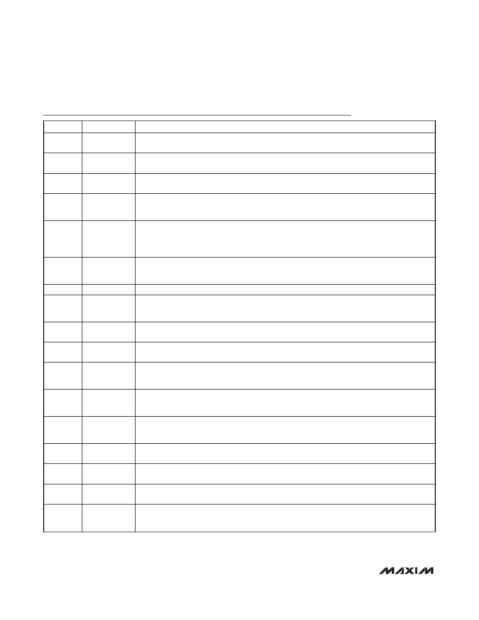
Pin Description
PIN
NAME
FUNCTION
1 P1.3/TCK
Port 1 Data 3/JTAG Serial Clock Input. P1.3 is a general-purpose digital I/O. TCK is the JTAG
serial test clock input. Refer to the MAXQ7667 User’s Guide Sections 5 and 11.
2 P1.4/MOSI
Port 1 Data 4/SPI Serial Data Output. P1.4 is a general-purpose digital I/O. MOSI is the master
output, slave input for the SPI interface. Refer to the MAXQ7667 User’s Guide Sections 5 and 9.
3 P1.5/MISO
Port 1 Data 5/SPI Serial Data Input. P1.5 is a general-purpose digital I/O. MISO is the master input,
slave output for the SPI interface. Refer to the MAXQ7667 User’s Guide Sections 5 and 9.
4 P1.6/SCLK
Port 1 Data 6/SPI Serial Clock Output. P1.6 is a general-purpose digital I/O. SCLK is the serial
clock for the SPI interface. SCLK is an input when operating as a slave and an output when
operating as a master. Refer to the MAXQ7667 User’s Guide Sections 5 and 9.
5 P1.7/SYNC/SS
Port 1 Data 7/Schedule Timer Sync Input/SPI Slave Select. P1.7 is a general-purpose digital I/O.
A rising edge on the SYNC input resets the schedule timer. In SPI slave mode, SS is the SPI
slave-select input. In SPI master mode, use SS or a GPIO to manually select an external slave.
Refer to the MAXQ7667 User’s Guide Sections 5, 7, and 9.
6, 19, 42
DVDD
Digital Supply Voltage. Connect DVDD directly to a +2.5V external source or to REG2P5 output for
single supply operation. Bypass DVDD to DGND with a 0.1µF capacitor as close as possible to
the device. Connect all DVDD nodes together.
7, 18, 43
DGND
Digital Ground. Connect all DGND nodes together. Connect to AGND at a single point.
8, 17, 44
DVDDIO
Digital I/O Supply Voltage. DVDDIO powers all digital I/Os except for XIN and XOUT. Bypass
DVDDIO to DGND with a 0.1µF capacitor as close as possible to the device. Connect all DVDDIO
nodes together.
9 P0.0/URX
Port 0 Data 0/UART Receive Data Input. P0.0 is a general-purpose digital I/O. URX is a UART or
LIN data receive input. Refer to the MAXQ7667 User’s Guide Sections 5 and 8.
10 P0.1/UTX
Port 0 Data 1/UART Transmit Data Output. P0.1 is a general-purpose digital I/O. UTX is a UART or
LIN data transmit output. Refer to the MAXQ7667 User’s Guide Sections 5 and 8.
11 P0.2/
TXEN
Port 0 Data 2/UART Transmit Output. P0.2 is a general-purpose digital I/O.
TXEN asserts low when
the UART is transmitting. Use
TXEN to enable an external LIN/UART transceiver. Refer to the
MAXQ7667 User’s Guide Sections 5 and 8.
12
P0.3/T0/
ADCCTL
Port 0 Data 3/Timer 0 I/O/ADC Control Input. P0.3 is a general-purpose digital I/O. T0 is the
primary Type 2 timer/counter 0 output or input. ADCCTL is a sampling/conversion trigger input for
the SAR ADC. Refer to the MAXQ7667 User’s Guide Sections 5, 6, and 14.
13 P0.4/T0B
Port 0 Data 4/Timer 0B I/O/Comparator Output. P0.4 is a general-purpose digital I/O. T0B is the
secondary Type 2 timer/counter 0 output or input. Refer to the MAXQ7667 User’s Guide Sections
5 and 6.
14 P0.5/T1
Port 0 Data 5/Timer 1 I/O. P0.5 is a general-purpose digital I/O. T1 is the primary Type 2
timer/counter 1 output or input. Refer to the MAXQ7667 User’s Guide Sections 5 and 6.
15 P0.6/T2
Port 0 Data 6/Timer 2 I/O. P0.6 is a general-purpose digital I/O. T2 is the primary Type 2
timer/counter 2 output or input. Refer to the MAXQ7667 User’s Guide Sections 5 and 6.
16 P0.7/T2B
Port 0 Data 7/Timer 2B I/O. P0.7 is a general-purpose digital I/O. T2B is the secondary Type 2
timer/counter 2 output or input. Refer to the MAXQ7667 User’s Guide Sections 5 and 6.
20 XIN
Crystal Oscillator Input. Connect an external crystal or resonator between XIN and XOUT. When
using an external clock source drive XIN with 2.5V level clock while leaving XOUT unconnected.
Connect XIN to DGND when an external clock source is not used.