Recommended dc operating conditions (continued) – Rainbow Electronics MAXQ2010 User Manual
Page 5
MAXQ2010
16-Bit Mixed-Signal Microcontroller with LCD
_______________________________________________________________________________________
5
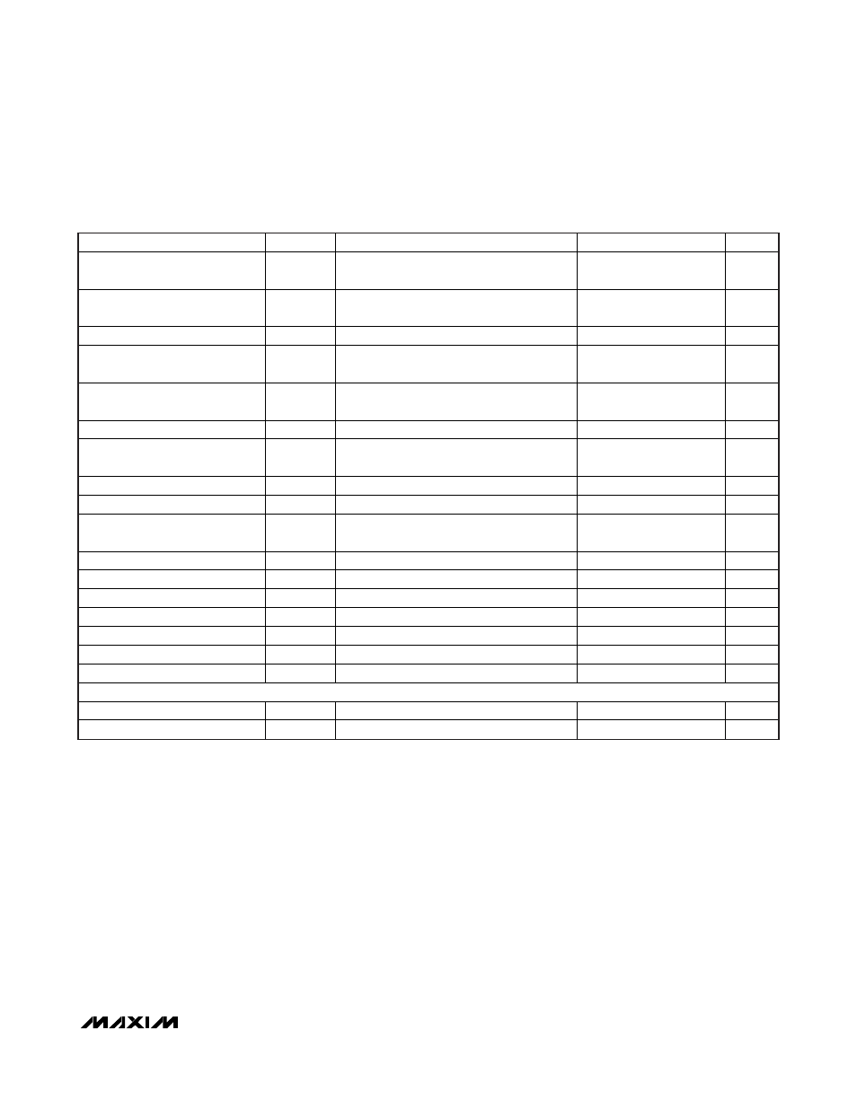
RECOMMENDED DC OPERATING CONDITIONS (continued)
(V
DVDD
= V
AVDD
= 2.7V to 3.6V, T
A
= -40°C to +85°C.) (Note 1)
PARAMETER SYMBOL
CONDITIONS
MIN
TYP
MAX
UNITS
Input High Voltage on HFXIN
and 32KIN
V
IH1
0.75 x
V
DVDD
V
DVDD
V
Input High Voltage on All Other
Pins
V
IH2
0.70
V
DVDD
V
DVDD
V
Input Hysteresis (Schmitt)
V
IHYS
0.18
V
Output Low Voltage for All Port
Pins (Note 10)
V
OL
I
OL
= +4mA
DGND
0.4
V
Output High Voltage for All Port
Pins (Note 10)
V
OH
I
OH
= -4mA
V
DVDD
- 0.4
V
I/O Pin Capacitance
C
IO
Guaranteed by design
15
pF
I/O Pin Capacitance SCL, SDA
(Note 11)
C
IO_I2C
Guaranteed by design
10
pF
RST Pullup Resistance
R
RST
30 85 k
Input Low Current for
RST Pin
I
IL1
V
IN
=
0.4V
-85 -30 μA
Input Low Current for All Other
Pins
I
IL2
V
IN
=
0.4V
-85 -30 μA
Input Leakage Current
I
L
Internal pullup disabled
-150
+150
nA
Input Pullup Resistor
R
PU
30 85 k
CLOCK SOURCE
External Clock Frequency
f
HFIN
DC
10 MHz
External Clock Period
t
CLCL
100
ns
External Clock Duty Cycle
t
XCLK_DUTY
40 60 %
System Clock Frequency
f
CK
DC
10 MHz
FREQUENCY-LOCKED LOOP (FLL)
FLL Output Frequency
f
FLL
f
32KIN
= 32.768kHz
8.4
MHz
FLL Output Frequency Delta
f
FLL
f
32KIN
= 32.768kHz
1.5
±5 %
Note 1:
Specifications to -40°C are guaranteed by design and are not production tested.
Note 2:
Typical value presented for reference only. Do not draw current from this pin.
Note 3:
FLL disabled. Crystal connected across HFXIN and HFXOUT. Operating in divide-by-1 mode. Measured on the DVDD pin
and part executing program code from flash. All inputs are connected to GND or DVDD. Outputs do not source/sink any
current. Timer B enabled.
Note 4:
This parameter is guaranteed by design and is not production tested.
Note 5:
FLL enabled. f
32KIN
= 32.768kHz, HFXIN = disconnected, FLL = 8.39MHz, measured on the DVDD pin, part executing
program code from flash. All inputs are connected to GND or DVDD. Outputs do not source/sink any current. Timer B
enabled.
Note 6:
I
STOP
is the total current into the device when the device is in stop mode. This includes both the digital and analog current
(current into DVDD and AVDD).
Note 7:
Regulator, brownout monitor, LCD, and RTC disabled.
Note 8:
Regulator, brownout monitor, and LCD disabled; RTC enabled.
Note 9:
Regulator enabled, brownout monitor enabled, and LCD and RTC disabled.
Note 10: I
OH(MAX)
+ I
OL(MAX)
for all outputs combined should not exceed 35mA to meet the specification.
Note 11: When DVDD is switched off, SDA and SCL may obstruct the line.