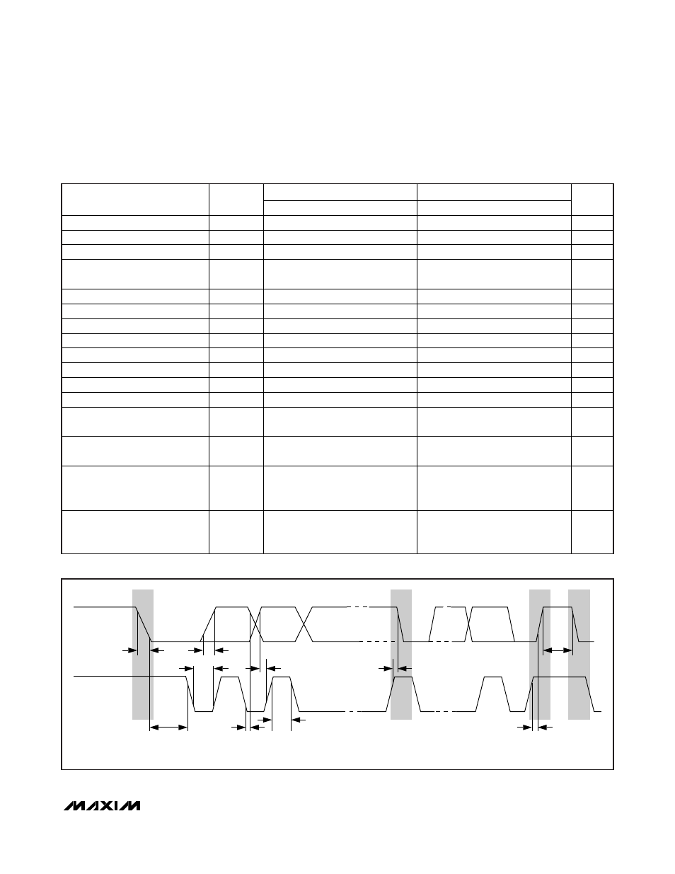
I2c bus controller timing (acting as i2c slave), C bus controller timing (acting as i, C slave) – Rainbow Electronics MAXQ2010 User Manual
Page 13: Figure 4. i, C bus controller timing diagram
MAXQ2010
16-Bit Mixed-Signal Microcontroller with LCD
______________________________________________________________________________________
13
I
2
C BUS CONTROLLER TIMING (ACTING AS I
2
C SLAVE)
(V
DVDD
= V
AVDD
= 2.7V to 3.6V, T
A
= -40°C to +85°C.) (Figure 4)
STANDARD MODE
FAST MODE
PARAMETER SYMBOL
MIN MAX MIN MAX
UNITS
System Frequency
f
SYS
0.9 3.60
MHz
Operating Frequency
f
I2C
f
SYS
/8 f
SYS
/8 Hz
System Clock Period
t
SYS
1/f
I2C
1/f
I2C
μs
Hold Time After (Repeated)
START
t
HD:STA
3t
SYS
3t
SYS
μs
Clock Low Period
t
LOW_I2C
5t
SYS
5t
SYS
μs
Clock High Period
t
HIGH_I2C
3t
SYS
3t
SYS
μs
Setup Time for Repeated START
t
SU:STA
5t
SYS
5t
SYS
μs
Hold Time for Data
t
HD:DAT
0
3.45
0
0.9 μs
Setup Time for Data
t
SU:DAT
250 100
ns
SDA/SCL Fall Time
t
F_I2C
300
20
+
0.1C
B
300 ns
SDA/SCL Rise Time
t
R_I2C
1000
20
+
0.1C
B
300 ns
Setup Time for STOP
t
SU:STO
3t
SYS
3t
SYS
μs
Bus-Free Time Between STOP
and START
t
BUF
5t
SYS
5t
SYS
μs
Capacitive Load for Each Bus
Line
C
B
400 400
pF
Noise Margin at the Low Level
for Each Connected Device
(Including Hysteresis)
V
NL_I2C
0.1
x
V
DVDD
0.1
x
V
DVDD
V
Noise Margin at the High Level
for Each Connected Device
(Including Hysteresis)
V
NH_I2C
0.2
x
V
DVDD
0.2
x
V
DVDD
V
SDA
SCL
S
SR
P
S
t
F_I2C
t
R_I2C
t
LOW
t
HIGH
t
HD:STA
t
SU:DAT
t
SU:STA
t
SU:STO
t
BUF
t
HD:DAT
NOTE: TIMING REFERENCED TO V
IH_I2C(MIN)
AND V
IL_I2C(MAX)
.
Figure 4. I
2
C Bus Controller Timing Diagram