Applications information, Table 2. required minimum capacitance values – Rainbow Electronics MAX13237E User Manual
Page 13
ESD Test Conditions
ESD performance depends on a variety of conditions.
Contact Maxim for a reliability report that documents
test setup, test methodology, and test results.
Human Body Model
Figure 8a shows the Human Body Model and Figure 8b
shows the current waveform it generates when dis-
charged into a low impedance. This model consists of
a 100pF capacitor charged to the ESD voltage of inter-
est, which is then discharged into the test device
through a 1.5kΩ resistor.
IEC 61000-4-2
The IEC 61000-4-2 standard covers ESD testing and
performance of finished equipment; it does not specifi-
cally refer to integrated circuits. The MAX13234E–
MAX13237E helps design equipment that meets Level
4 (the highest level) of IEC 61000-4-2, without the need
for additional ESD-protection components. The major
difference between tests done using the Human Body
Model and IEC 61000-4-2 is higher peak current in IEC
61000-4-2, because series resistance is lower in the
IEC 61000-4-2 model. Hence, the ESD withstand volt-
age measured to IEC 61000-4-2 is generally lower than
that measured using the Human Body Model. Figure 9a
shows the IEC 61000-4-2 model and Figure 9b shows
the current waveform for the 8kV, IEC 61000-4-2, Level
4, ESD Contact-Discharge Method.
The Air-Gap Method involves approaching the device
with a charged probe. The Contact-Discharge Method
connects the probe to the device before the probe is
energized.
Applications Information
Capacitor Selection
The capacitor type used for C1–C4 is not critical for
proper operation; polarized or non-polarized capacitors
can be used. The charge pump requires 0.1µF capaci-
tors for V
CC
= +3.3V operation. For other supply volt-
ages, see Table 2 for required capacitor values. Do not
use values smaller than those listed in Table 2.
Increasing the capacitor values (e.g., by a factor of 2)
reduces ripple on the transmitter outputs and slightly
reduces power consumption. C2, C3, and C4 can be
increased without changing C1’s value. However, do
not increase C1 without also increasing the values
of C2, C3, C4, C
BYPASS1
, and C
BYPASS2
to maintain
the proper ratios (C1 to the other capacitors). When
using the minimum required capacitor values, make
sure the capacitor value does not degrade excessively
with temperature. If in doubt, use capacitors with a
larger nominal value. The capacitor’s equivalent series
resistance (ESR), usually rises at low temperatures
influencing the amount of ripple on V+ and V-.
Power-Supply Decoupling
In most circumstances, a 0.1µF V
CC
bypass capacitor
and a 1µF V
L
bypass capacitor are adequate. In appli-
cations that are sensitive to power-supply noise, use
capacitors of the same value as charge-pump capaci-
tor C1. Connect bypass capacitors as close to the IC
as possible.
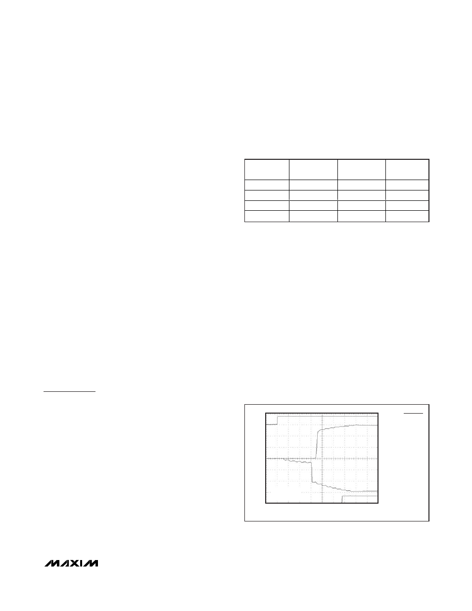
Transmitter Outputs when Exiting
Shutdown
Figure 10 shows two transmitter outputs when exiting
shutdown mode. As they become active, the two trans-
mitter outputs are shown going to opposite RS-232 lev-
els (one transmitter input is high, the other is low). Each
transmitter is loaded with 3kΩ in parallel with 1000pF.
The transmitter outputs display no ringing or undesir-
able transients as they come out of shutdown. Note that
the transmitters are enabled only when the magnitude
of V- exceeds approximately -3V.
MAX13234E–MAX13237E
3Mbps RS-232 Transceivers with
Low-Voltage Interface
______________________________________________________________________________________
13
V
CC
(V)
C1, C
BYPASS2
(µF)
C
BYPASS1
(µF)
C2, C3, C4
(µF)
3.0 to 3.6
0.22
0.22
0.22
3.15 to 3.6
0.1
0.1
0.1
4.5 to 5.5
0.047
1
0.33
3.0 to 5.5
0.22
1
1
Table 2. Required Minimum Capacitance
Values
5
μs/div
T1OUT
FORCEON = FORCEOFF
T2OUT
READY
5V/div
0
2V/div
0
5V/div
0
V
CC
= 3.3V
C1–C4 = 0.1
μF
Figure 10. Transmitter Outputs when Exiting Shutdown or
Powering Up