Electrical characteristics, Absolute maximum ratings – Rainbow Electronics MAX17127 User Manual
Page 2
2 ______________________________________________________________________________________
MAX17127
Six-String WLED Driver with Integrated
Step-Up Converter
Stresses beyond those listed under “Absolute Maximum Ratings” may cause permanent damage to the device. These are stress ratings only, and functional
operation of the device at these or any other conditions beyond those indicated in the operational sections of the specifications is not implied. Exposure to absolute
maximum rating conditions for extended periods may affect device reliability.
V
IN
to AGND ........................................................-0.3V to +30V
FB_, SW to PGND .................................................-0.3V to +52V
PGND to AGND ....................................................-0.3V to +0.3V
V
DDIO
, PWM, EN, FPO, I.C. to AGND .....................-0.3V to +6V
COMP, ISET, R_FPWM, OVP, FSLCT
to AGND ................................................-0.3V to V
DDIO
+ 0.3V
SW Switch Maximum Continuous RMS Current ...................1.6A
Continuous Power Dissipation (T
A
= +70NC)
TQFN (derate 16.9mW/NC above +70NC) ..................1349mW
Operating Temperature Range .......................... -40NC to +85NC
Junction Temperature .....................................................+150NC
Storage Temperature Range ............................ -60NC to +150NC
ESD
HBM ................................................................................... 2kV
MM ...................................................................................200V
Lead Temperature (soldering, 10s) ................................+300NC
Soldering Temperature (reflow) ......................................+260NC
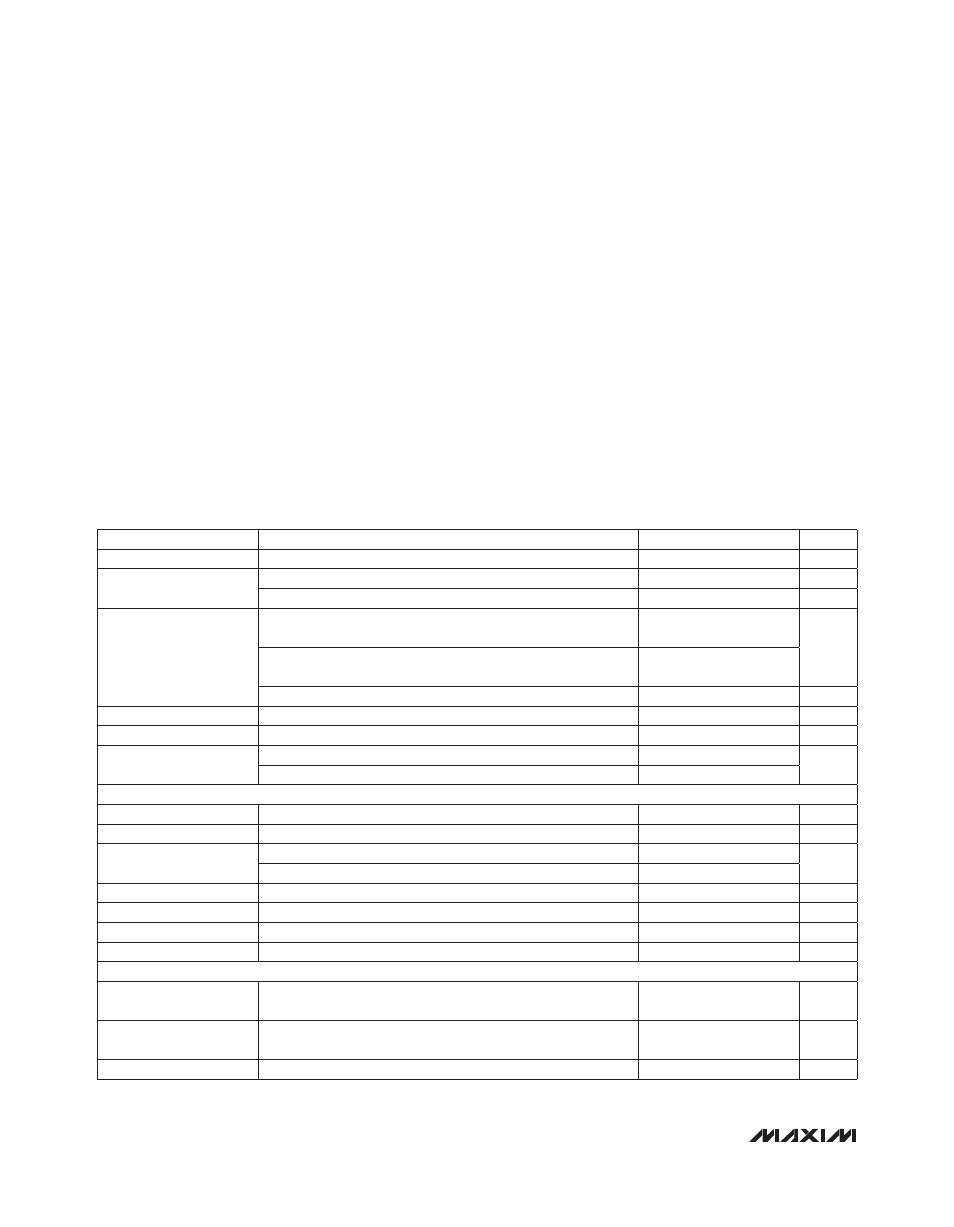
ELECTRICAL CHARACTERISTICS
(Circuit of Figure 1. V
IN
= 12V, C
COMP
= 0.51nF, C
COUT
= 4.7µF, R
COMP
= 82.5kΩ, R
ISET
= 180kΩ, R
FSLCT
= 100kΩ, L = 10µH,
T
A
= 0°C to +85°C, unless otherwise noted. Typical values are at T
A
= +25°C.)
ABSOLUTE MAXIMUM RATINGS
PARAMETER
CONDITIONS
MIN
TYP
MAX
UNITS
V
IN
Input Voltage Range
5
26
V
V
IN
Quiescent Current
MAX17127 is enabled, V
EN
= 3.3V, V
IN
= 26V
2.7
3.2
mA
MAX17127 is disabled, EN = AGND
5
10
F
A
V
DDIO
Output Voltage
MAX17127 is enabled, V
EN
= 3.3V,
5.4V < V
IN
< 26V, 0A < I
VDDIO
< 10mA
4.85
5
5.15
V
MAX17127 is enabled, V
EN
= 3.3V, V
IN
= 5V, I
VDDIO
= 10mA,
dropout condition
4.6
4.75
MAX17127 is disabled, EN = AGND, 0A < I
VDDIO
< 50FA
3.1
3.7
4.1
V
V
DDIO
Current Limit
V
DDIO
is forced to 4.2V
25
45
70
mA
V
DDIO
UVLO Threshold
Rising edge, typical hysteresis = 250mV
3.90
4.00
4.10
V
V
IN
UVLO Threshold
Falling edge
4.3
4.5
4.7
V
Rising edge
4.55
4.75
4.95
BOOST CONVERTER
SW On-Resistance
20mA from SW to PGND
0.12
0.25
I
SW Leakage Current
40V on SW, T
A
= +25NC
1
F
A
Operating Frequency
R
FSLCT
= 100kI
0.95
1.0
1.05
MHz
R
FSLCT
= 400kI
0.225
0.25
0.275
R
FSLCT
Range
Operating range
90
500
kI
Maximum Duty Cycle
At f
SW
= 1MHz
91
95
%
Minimum On-Time
(Note 1)
50
80
ns
SW Current Limit
Duty cycle = 75%
3.12
3.9
4.7
A
CONTROL INPUT
PWM, EN Logic-Input
High Level
2.1
V
PWM, EN Logic-Input Low
Level
0.8
V
EN Pulldown Resistor
120
200
280
kI