Rainbow Electronics MAX66020 User Manual
Page 10
MAX66020
the block number field. The block number is used to
ensure that the response received relates to the
request sent. This function is important in the error han-
dling, which is illustrated in Annex B of ISO/IEC 14443-
4. The rules that govern the numbering and handling of
blocks are found in Sections 7.5.3 and 7.5.4 of
ISO/IEC 14443-4. The MAX66020 ignores I-blocks that
have bit 5 or bit 3 set to 1.
For R-blocks, the states of bit 2, bit 3, bit 6, bit 7, and
bit 8 are fixed and must be transmitted as shown in
Figure 13. The function of bit 1 (block number) and bit 4
(CID indicator) is the same as for I-blocks. Bit 5,
marked as AN, is used to acknowledge (if transmitted
as 0) or not to acknowledge (if transmitted as 1) the
reception of the last frame for recovery from certain
error conditions. The MAX66020 fully supports the func-
tion of the R-block as defined in the standard. For
details and the applicable rules, refer to Sections 7.5.3
and 7.5.4 and Annex B of ISO/IEC 14443-4.
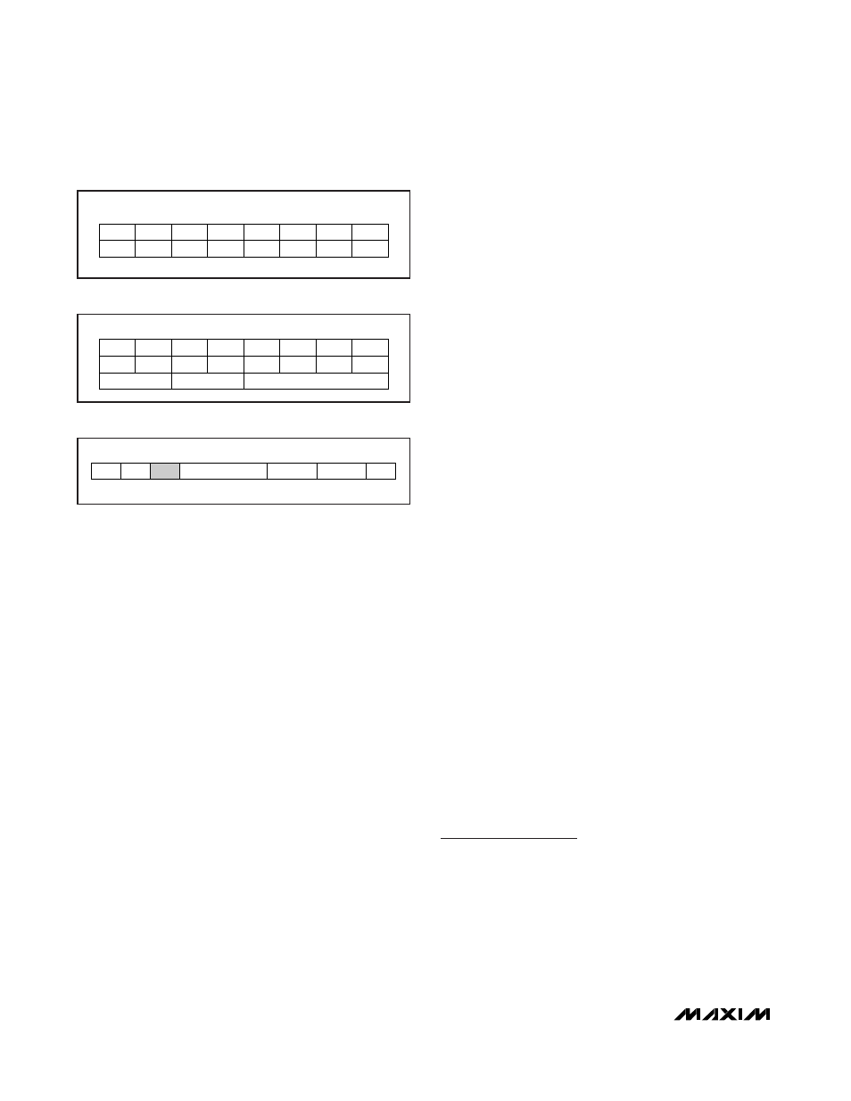
For S-blocks, the states of bit 1, bit 2, bit 3, and bit 7
and bit 8 are fixed and must be transmitted as shown in
Figure 14. The function of bit 4 (CID indicator) is the
same as for I-blocks. Bit 5 and bit 6, when 00b, specify
whether the S-block represents a deselect command. If
bit 5 and bit 6 are 11b, the S-block represents a frame-
waiting time extension (WTX) request, a feature to tell
the master that the response is going to take longer than
specified by the frame-waiting time (FWT) (see the
ATQB Response
section). However, the MAX66020
does not use this feature and consequently, the only use
of the S-block is to transition the device from the ACTIVE
state to the HALT state using the DESELECT command
(see the
Network Function Commands
section).
Card Identifier
Figure 15 shows the bit assignment within the card
identifier byte. The purpose of bits 4 to 1 is to select
one of multiple slave devices that the master has ele-
vated to the ACTIVE state. The CID is assigned to a
slave through Param 4 of the ATTRIB command (see
the
Network Function Commands
section). While in
ACTIVE state, a compliant slave only processes blocks
that contain a matching CID and blocks without CID if
the assigned CID is all zeros. If the master includes a
CID, then the slave’s response also includes a CID
byte. Blocks with a nonmatching CIDs are ignored.
According to the standard, the slave can use bits 8 and
7 to inform the master whether power-level indication is
supported, and, if yes, whether sufficient power is avail-
able for full functionality. Since the MAX66020 does not
support power-level indication, the power-level bits are
always 00b. When the master transmits a CID byte, the
power-level bits must be 00b.
Information Field
Since the MAX66020 does not generate WTX requests,
the information field (Figure 11) is found only with
I-blocks. The length of the information field is calculated
by counting the number of bytes of the whole block
minus length of prologue and epilogue field. The
ISO/IEC 14443 standard does not define any rules for
the contents of the information field. The MAX66020
assumes that the first byte it receives in the information
field is a command code followed by 0 or more com-
mand-specific parameters. When responding to an
I-block, the first byte of the information field indicates
success (code 00h) followed by command-specific
data or failure (code 01h) followed by one error code.
Memory and Control
Function Commands
The commands described in this section are transmit-
ted using the block transmission protocol. The data of a
block (from prologue to epilogue) is embedded
between SOF and EOF, as shown in Figure 16. The CID
field (shaded) is optional. If the request contains a CID,
the response also contains a CID.
ISO/IEC 14443 Type B-Compliant
1Kb Memory Fob
10
______________________________________________________________________________________
BIT 8
BIT 7
BIT 6
BIT 5
BIT 4
BIT 3
BIT 2
BIT 1
MSb
LSb
1
1
CID
0
1
0
Figure 14. Bit Assignments for S-Block PCB
BIT 8
BIT 7
BIT 6
BIT 5
BIT 4
BIT 3
BIT 2
BIT 1
MSb
LSb
0
0
0
0
(POWER LEVEL)
(FIXED)
CARD IDENTIFIER VALUE
Figure 15. Bit Assignments for CID Byte in I-Blocks
PCB
CID
SOF
INFORMATION FIELD
CRC (MSB)
CRC (LSB)
EOF
Figure 16. Frame Format for Block Transmission Protocol