Max8707 – Rainbow Electronics MAX8707 User Manual
Page 22
MAX8707
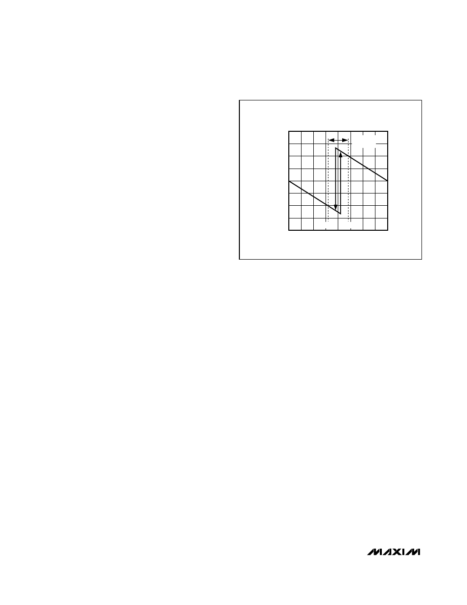
to 2V, the offset amplifier adds a positive offset to the
output that is equal to 1/8th the difference between the
reference voltage and the voltage appearing at the
OFS input (V
OFFSET
= 0.125 x (V
REF
- V
OFS
)). With this
scheme, the controller supports both positive and neg-
ative offsets with a single input. The piecewise linear-
transfer function is shown in
Figure
3. The regions of
the transfer function below zero, above 2.0V, and
between 0.8V and 1.2V are undefined. OFS inputs are
disallowed in these regions, and the respective effects
on the output are not specified.
The controller disables the offset amplifier during sus-
pend mode (SUS = high).
Nominal Output-Voltage Selection
The nominal no-load output voltage (V
TARGET
) is defined
by the selected voltage reference (VID DAC or SUSV)
plus the offset voltage and remote ground-sense adjust-
ment (V
GNDS
) as defined in the following equation:
V
TARGET
= V
DAC
+ V
OFFSET
+ V
GNDS
when SUS = GND
where V
DAC
is the selected VID voltage during normal
operation (SUS = low,
Table
4), and V
OFFSET
is the offset
voltage defined by the OFS pin (
Figure
3). In suspend
mode (SUS = high), the offset voltage amplifier is disabled
and the target voltage tracks the SUSV input voltage:
V
TARGET
= V
SUSV
+ V
GNDS
when SUS = V
CC
The MAX8707 uses a multiplexer that selects from one of
three different inputs (
Figure
2)—the output of the VID
DAC, the SUSV suspend voltage, or ground (controller
disabled). On startup, the MAX8707 slews the target volt-
age from ground to either the decoded D0–D4 (SUS =
low) voltage or the SUSV voltage (SUS = high).
DAC Inputs (D0–D4)
During normal forced-PWM operation (SUS = low), the
DAC programs the output voltage using the D0–D4
inputs. D0–D4 are low-voltage (1.0V) logic inputs,
designed to interface directly with the CPU. Do not leave
D0–D4 unconnected. D0–D4 can be changed while the
MAX8707 is active, initiating a transition to a new output-
voltage level. Change D0–D4 together, avoiding greater
than 50ns skew between bits. Otherwise, incorrect DAC
readings may cause a partial transition to the wrong volt-
age level followed by the intended transition to the cor-
rect voltage level, lengthening the overall transition time.
The available DAC codes and resulting output voltages
are compatible with the AMD Hammer (
Table
4) specifi-
cations.
Suspend Mode
When the processor enters low-power suspend mode,
the processor sets the regulator to a lower output voltage
to reduce power consumption. The MAX8707 includes a
buffered suspend-voltage input (SUSV) and a digital
SUS control input. The suspend voltage is adjusted with
an external resistive voltage-divider from REF to SUSV to
analog ground. The suspend-voltage adjustment range
is from 0.4V to 2.0V (V
REF
).
When the CPU suspends operation (SUS = high), the
controller disables the offset amplifier, overrides the 5-bit
VID-DAC code set by D0–D4, and slews the output volt-
age to the target voltage set by the SUSV voltage. During
the transition, the MAX8707 blanks both VROK thresh-
olds until 20µs after the slew-rate controller reaches the
suspend-mode voltage. Once the 20µs timer expires, the
MAX8707 (SKIP pulled low) automatically switches to the
1-phase, pulse-skipping control scheme, forces DRSKP
low, and blanks the upper VROK threshold.
Output-Voltage Transition Timing
The MAX8707 performs mode transitions in a controlled
manner, automatically minimizing input surge currents.
This feature allows the circuit designer to achieve nearly
Multiphase, Fixed-Frequency Controller for
AMD Hammer CPU Core Power Supplies
22
______________________________________________________________________________________
OUTPUT OFFSET VOLTAGE
vs. OFS INPUT VOLTAGE
OFS VOLTAGE (V
OFS
)
OUTPUT OFFSET VOLTAGE
1.5V
0.5V
1.0V
-100mV
0
100mV
200mV
-200mV
0
2.0V
0.8V
1.2V
UNDEFINED
REGION
Figure
3. Output Offset Voltage vs. OFS Input Voltage