Absolute maximum ratings, Electrical characteristics – Rainbow Electronics MAX8707 User Manual
Page 2
MAX8707
Multiphase, Fixed-Frequency Controller for
AMD Hammer CPU Core Power Supplies
2
_______________________________________________________________________________________
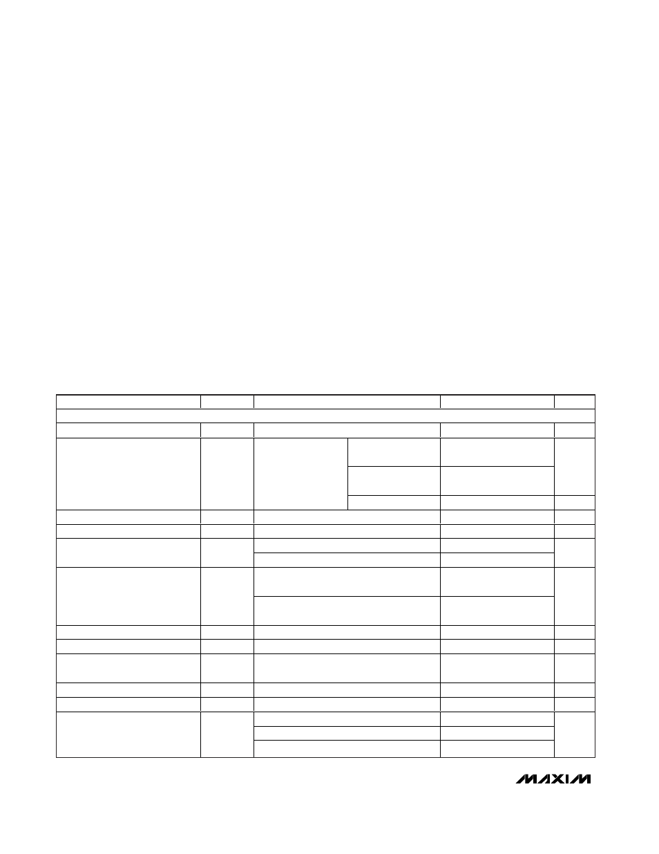
ABSOLUTE MAXIMUM RATINGS
Stresses beyond those listed under “Absolute Maximum Ratings” may cause permanent damage to the device. These are stress ratings only, and functional
operation of the device at these or any other conditions beyond those indicated in the operational sections of the specifications is not implied. Exposure to
absolute maximum rating conditions for extended periods may affect device reliability.
V
CC
to GND ..............................................................-0.3V to +6V
D0–D4 to GND..........................................................-0.3V to +6V
SKIP, SUS, VROK, ILIM(AVE) to GND......................-0.3V to +6V
SUSV, OFS, OSC to GND.........................................-0.3V to +6V
CSP_, CSN_, CRSP, CRSN to GND .........................-0.3V to +6V
VPS, FBS, CCV, REF to GND .....................-0.3V to (V
CC
+ 0.3V)
ILIM(PK), TRC, TIME to GND .....................-0.3V to (V
CC
+ 0.3V)
PWM_,
DRSKP to PGND ............................-0.3V to (V
CC
+ 0.3V)
PGND, GNDS to GND ...........................................-0.3V to +0.3V
SHDN to GND (Note 1)...........................................-0.3V to +14V
REF Short-Circuit Duration .........................................Continuous
Continuous Power Dissipation (T
A
= +70°C)
40-Pin 6mm x 6mm Thin QFN
(derate 26.3mW/°C above +70°C) ................................2.105W
Operating Temperature Range ...........................-40°C to +85°C
Junction Temperature ......................................................+150°C
Storage Temperature Range .............................-65°C to +150°C
Lead Temperature (soldering, 10s) .................................+300°C
ELECTRICAL CHARACTERISTICS
(Circuit of Figure 1. V
CC
= V
SHDN
= 5V, OSC = REF, V
VPS
= V
FBS
= V
CRSN
= V
CRSP
= V
CSP_
= 1.20V, V
SUSV
= 0.8V, OFS = SUS =
GNDS = PGND = SKIP = GND, D0–D4 set for 1.20V (D0–D4 = 01110). T
A
= 0°C to +85°C, unless otherwise specified. Typical values
are at T
A
= +25°C.)
PARAMETER
SYMBOL
CONDITIONS
MIN
TYP
MAX
UNITS
PWM CONTROLLER
Input Voltage Range
V
CC
4.5
5.5
V
DAC codes from
1.10V to 1.55V
-0.75
+0.75
DAC codes from
0.80V to 1.075V
-2.0
+2.0
%
DC Output Voltage Accuracy
V
OUT
Includes load-
regulation error
(VPS = FBS)
SUS = V
CC
-20
+20
mV
SUSV Input Range
V
SUSV
0.4
2.0
V
SUSV Input-Bias Current
I
SUSV
V
SUSV
= 0.4V to 2V
-0.1
+0.1
µA
Negative offsets
0
0.8
OFS Input Range
V
OFS
Positive offsets
1.2
2.0
V
∆V
OUT
/
∆V
OFS
,
∆V
OFS
= V
OFS
,
V
OFS
= 0 to 0.8V
-0.131
-0.125
-0.118
OFS GAIN
A
OFS
∆V
OUT
/
∆V
OFS
,
∆V
OFS
= V
OFS
-V
REF
,
V
OFS
= 1.2V to 2V
-0.131
-0.125
-0.118
V/V
OFS Input-Bias Current
I
OFS
V
OFS
= 0 to 2V
-0.1
+0.1
µA
GNDS Input Range
V
GNDS
-200
+200
mV
GNDS Gain
A
GNDS
∆V
OUT
/
∆V
GNDS
,
-200mV
≤ V
GNDS
≤ +200mV
0.95
1.00
1.05
V/V
GNDS Input-Bias Current
I
GNDS
-2
+2
µA
FBS Input-Bias Current
I
FBS
CRSP = CRSN, CSP_ = CSN_
-10
+10
µA
OSC = GND
180
200
220
OSC = REF
270
300
330
Switching Frequency Accuracy
(Per Phase)
f
SW
OSC = V
CC
540
600
660
kHz
Note 1: SHDN can be forced to 12V for debugging prototype boards using the no-fault test mode, which disables fault protection.