Pin description (continued) – Rainbow Electronics MAX6871 User Manual
Page 9
MAX6870/MAX6871
EEPROM-Programmable Hex/Quad
Power-Supply Sequencers/Supervisors with ADC
_______________________________________________________________________________________
9
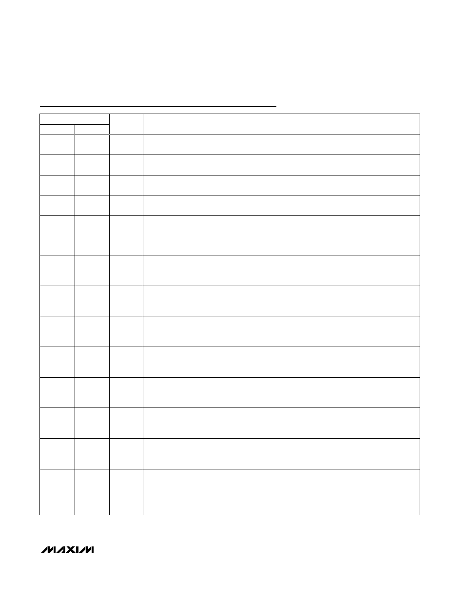
Pin Description (continued)
PIN
MAX6870
MAX6871
NAME
FUNCTION
17
17
GPI4
General-Purpose Logic Input 4. An internal 10µA current source pulls GPI4 to GND. Configure
GPI4 to control watchdog timer functions or the programmable outputs.
18
18
GPI3
General-Purpose Logic Input 3. An internal 10µA current source pulls GPI3 to GND. Configure
GPI3 to control watchdog timer functions or the programmable outputs.
19
19
GPI2
General-Purpose Logic Input 2. An internal 10µA current source pulls GPI2 to GND. Configure
GPI2 to control watchdog timer functions or the programmable outputs.
20
20
GPI1
General-Purpose Logic Input 1. An internal 10µA current source pulls GPI1 to GND. Configure
GPI1 to control watchdog timer functions or the programmable outputs.
21
21
ABP
Internal Power-Supply Output. Bypass ABP to GND with a 1µF ceramic capacitor. ABP powers
the internal circuitry of the MAX6870/MAX6871. ABP supplies the input voltage to the internal
charge pumps when the programmable outputs are configured as charge-pump outputs. Do
not use ABP to supply power to external circuitry.
22
22
DBP
Internal Digital Power-Supply Output. Bypass DBP to GND with a 1µF ceramic capacitor. DBP
supplies power to the EEPROM memory and the internal logic circuitry. Do not use DBP to
supply power to external circuitry.
23
23
AUXIN2
Auxiliary Input 2. A 10-bit ADC monitors the input voltage at AUXIN2. The high-impedance
AUXIN2 input accepts input voltages up to V
REFIN
. AUXIN2 does not influence EEPROM-
configurable power-supply sequencing or reset detection functions.
24
24
AUXIN1
Auxiliary Input 1. A 10-bit ADC monitors the input voltage at AUXIN1. The high-impedance
AUXIN1 input accepts input voltages up to V
REFIN
. AUXIN1 does not influence EEPROM-
configurable power-supply sequencing or reset detection functions.
25
—
IN6
Voltage Input 6. Configure IN6 to detect voltage thresholds between +1V and +5.5V in 20mV
increments, or +0.5V to +3.05V in 10mV increments. For improved noise immunity, bypass IN6
to GND with a 0.1µF capacitor installed as close to the device as possible.
26
—
IN5
Voltage Input 5. Configure IN5 to detect voltage thresholds between +1V and +5.5V in 20mV
increments, or +0.5V to +3.05V in 10mV increments. For improved noise immunity, bypass IN5
to GND with a 0.1µF capacitor installed as close to the device as possible.
27
27
IN4
Voltage Input 4. Configure IN4 to detect voltage thresholds between +1V and +5.5V in 20mV
increments, or +0.5V to +3.05V in 10mV increments. For improved noise immunity, bypass IN4
to GND with a 0.1µF capacitor installed as close to the device as possible.
28
28
IN3
Voltage Input 3. Configure IN3 to detect voltage thresholds between +1V and +5.5V in 20mV
increments, or +0.5V to +3.05V in 10mV increments. For improved noise immunity, bypass IN3
to GND with a 0.1µF capacitor installed as close to the device as possible.
29
29
IN2
Bipolar Voltage Input 2. Configure IN2 to detect negative voltage thresholds from -2.5V to
-15.25V in 50mV increments or -1.25V to -7.625V in 25mV increments. Alternatively, configure
IN2 to detect positive voltage thresholds from +2.5V to +15.25V in 50mV increments or +1.25V
to +7.625V in 25mV increments. For improved noise immunity, bypass IN2 to GND with a 0.1µF
capacitor installed as close to the device as possible.