Rainbow Electronics MAX6871 User Manual
Page 2
MAX6870/MAX6871
EEPROM-Programmable Hex/Quad
Power-Supply Sequencers/Supervisors with ADC
2
_______________________________________________________________________________________
ABSOLUTE MAXIMUM RATINGS
ELECTRICAL CHARACTERISTICS
(V
IN1
= +6.5V to +13.2V, V
IN2
= +10V, V
IN3
to V
IN6
= +2.7V to +5.5V, AUXIN_ = GPI_ = GND,
MARGIN = MR = DBP, T
A
= -40°C to
+85°C, unless otherwise noted. Typical values are at T
A
= +25°C.) (Notes 1 and 2)
Stresses beyond those listed under “Absolute Maximum Ratings” may cause permanent damage to the device. These are stress ratings only, and functional
operation of the device at these or any other conditions beyond those indicated in the operational sections of the specifications is not implied. Exposure to
absolute maximum rating conditions for extended periods may affect device reliability.
All Voltages referenced to GND
IN3–IN6, ABP, SDA, SCL, A0, A1,
GPI1–GPI4, MR, MARGIN, PO5–PO8
(MAX6870), PO3/PO4/PO5 (MAX6871)............-0.3V to +6V
IN1, PO1–PO4 (MAX6870), PO1/PO2 (MAX6871)....-0.3V to +14V
IN2 ...........................................................................-20V to +20V
DBP, AUXIN1, AUXIN2, REFIN.................................-0.3V to +3V
Input/Output Current (all pins)..........................................±20mA
Continuous Power Dissipation (T
A
= +70°C)
32-Pin 7mm x 7mm Thin QFN
(derate 33.3mW/°C above +70°C) .............................2667mW
Operating Temperature Range ...........................-40°C to +85°C
Maximum Junction Temperature .....................................+150°C
Storage Temperature Range .............................-65°C to +150°C
Lead Temperature (soldering, 10s) .................................+300°C
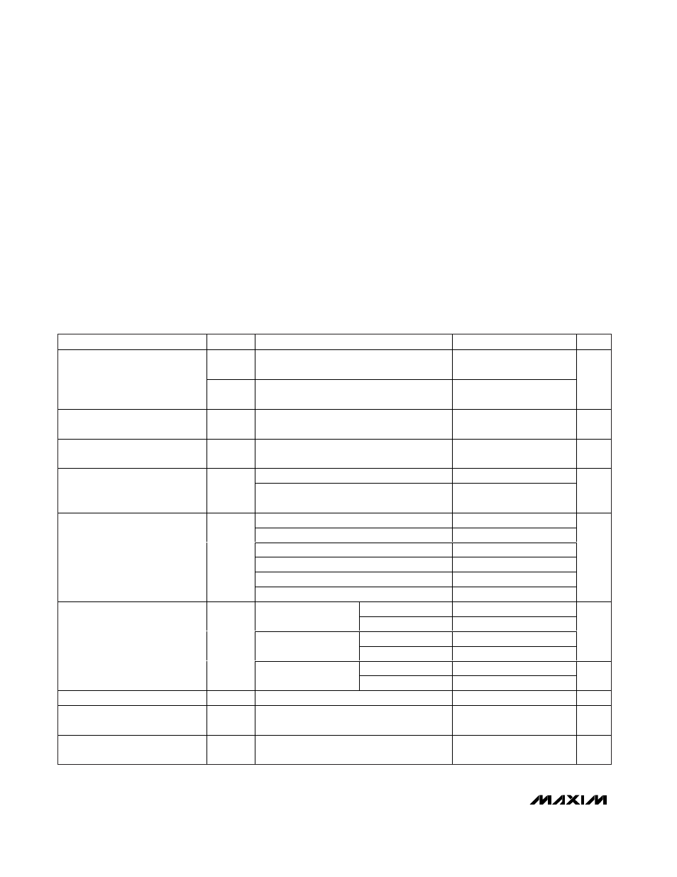
PARAMETER
SYM B O L
CONDITIONS
MIN
TYP
MAX
UNITS
V
IN1
Voltage on IN1 to ensure the device is fully
operational, IN3 to IN6 = GND
4.0
13.2
Operating Voltage Range
(Note 3)
V
IN3
to
V
IN6
Voltage on any one of IN3 to IN6 to ensure
the device is fully operational, IN1 = GND
2.7
5.5
V
IN1 Supply Voltage
(Note 3)
V
IN1P
Minimum voltage on IN1 to guarantee that the
device is powered through IN1
6.5
V
Undervoltage Lockout
V
UVLO
Minimum voltage on one of IN3 to IN6 to
guarantee the device is EEPROM configured.
2.5
V
V
IN1
= +13.2V, IN2 to IN6 = GND, no load
1.2
1.5
Supply Current
I
CC
Writing to configuration registers or EEPROM,
no load
1.3
2
mA
V
IN1
(50mV increments)
2.5
13.2
V
IN1
(25mV increments)
1.250
7.625
V
IN2
(50mV increments)
±2.50
±15.25
V
IN2
(25mV increments)
±1.250
±7.625
V
IN3
to V
IN6
(20mV increments)
1.0
5.5
Threshold Range
V
TH
V
IN3
to V
IN6
(10mV increments)
0.50
3.05
V
T
A
= +25°C
-1.0
+1.0
IN1 to IN6 positive,
V
IN_
falling
T
A
= -40°C to +85°C
-1.5
+1.5
T
A
= +25°C
-1.5
+1.5
-15.25V
≤ V
IN2
≤ -5V,
V
IN2
falling
T
A
= -40°C to +85°C
-2
+2
%
T
A
= +25°C
-75
+75
Threshold Accuracy
-5V
≤ V
IN2
≤ 0, V
IN2
falling
T
A
= -40°C to +85°C
-100
+100
mV
Threshold Hysteresis
V
TH-HYST
0.3
% V
TH
Reset Threshold Temperature
Coefficient
∆V
TH
/°C
10
ppm/
°C
Threshold-Voltage Differential
Nonlinearity
V
TH
DNL
-1
+1
LSB