Table 25. po_ timeout periods – Rainbow Electronics MAX6871 User Manual
Page 33

MAX6870/MAX6871
EEPROM-Programmable Hex/Quad
Power-Supply Sequencers/Supervisors with ADC
______________________________________________________________________________________
33
Charge-Pump Output Configuration
Configure the programmable outputs of the MAX6870/
MAX6871 as charge-pump outputs to drive n-channel
FETs for power-supply sequencing applications. Only
PO1–PO4 (MAX6870) or PO1 and PO2 (MAX6871) can be
configured as charge-pump output stages. The charge-
pump output high voltage is typically V
ABP
+5.5V when unloaded.
Push-Pull Output Configuration
The MAX6870/MAX6871’s programmable outputs sink
4mA and source 10mA when configured as push-pull
outputs. Only PO5–PO8 (MAX6870), or PO3/PO4/PO5
(MAX6871) can be configured as push-pull output
stages. The push-pull output stages refer to any of
IN3–IN6 (MAX6870)/IN3/IN4 (MAX6871) as configured
in Tables 23 and 24. Use the push-pull output configu-
ration to drive loads with fast rise/fall times, or those
with low impedance.
Weak Pullup Output Configuration
The MAX6870/MAX6871’s programmable outputs sink
4mA when configured as weak pullups. The weak pullup
of 10k
Ω refers to any of IN3–IN6 (MAX6870)/IN3/IN4
(MAX6871) or ABP as configured in Tables 23 and 24.
All programmable outputs of the MAX6870/MAX6871
may be configured as weak pullups.
Open-Drain Output Configuration
Connect an external pullup resistor from the program-
mable output to an external voltage when configured as
an open-drain output. PO1–PO4 (PO1 and PO2 for the
MAX6871) may be pulled up to +13.2V. PO5–PO8
(PO3–PO5 for the MAX6871) may be pulled up to a
voltage less than or equal to ABP. Choose the pullup
resistor depending on the number of devices connect-
ed to the open-drain output and the allowable current
consumption. The open-drain output configuration
allows wire-ORed connections, and provides flexibility
in setting the pullup current.
Configuring the MAX6870/MAX6871
The MAX6870/MAX6871 factory-default configuration
sets all registers to 00h except 3Ah, which is set to FFh.
Each device requires configuration before full power is
applied to the system. To configure the MAX6870/
MAX6871, first apply an input voltage to IN1 or one of
IN3–IN6 (MAX6870)/IN3/IN4 (MAX6871) (see the
Powering the MAX6870/MAX6871 section). V
IN1
> +4V
or one of V
IN3
–V
IN6
> +2.7V, to ensure device operation.
Next, transmit data through the serial interface. Use the
block write protocol to quickly configure the device. Write
to the configuration registers first to ensure the device is
configured properly. After completing the setup proce-
dure, use the read word protocol to verify the data from
the configuration registers. Lastly, use the write word
protocol to write this data to the EEPROM registers. After
completing EEPROM register configuration, apply full
power to the system to begin normal operation. The non-
volatile EEPROM stores the latest configuration upon
removal of power. Write 0’s to all EEPROM registers to
clear the memory.
Software Reboot
A software reboot allows the user to restore the
EEPROM configuration to the volatile registers without
cycling the power supplies. Use the send byte com-
mand with data byte 88h to initiate a software reboot.
The 3.5ms (max) power-up delay also applies after a
software reboot.
SMBus/I
2
C-Compatible Serial Interface
The MAX6870/MAX6871 feature an I
2
C/SMBus-compati-
ble serial interface consisting of a serial data line (SDA)
and a serial clock line (SCL). SDA and SCL allow bidirec-
tional communication between the MAX6870/MAX6871
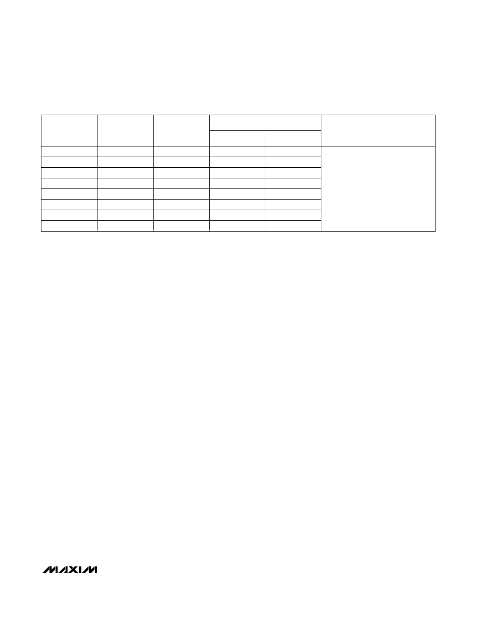
Table 25. PO_ Timeout Periods
AFFECTED OUTPUTS
REGISTER
ADDRESS
EEPROM
MEMORY
ADDRESS
BIT RANGE
MAX6870
MAX6871
DESCRIPTION
11h
8011h
[3:1]
PO1
—
15h
8015h
[3:1]
PO2
—
1Ch
801Ch
[4:2]
PO3
PO1
23h
8023h
[4:2]
PO4
PO2
2Ah
802Ah
[3:1]
PO5
PO3
31h
8031h
[3:1]
PO6
PO4
35h
8035h
[3:1]
PO7
PO5
39h
8039h
[3:1]
PO8
—
000 = 25µs
001 = 1.5625ms
010 = 6.25ms
011 = 25ms
100 = 50ms
101 = 200ms
110 = 400ms
111 = 1600ms
