Table 6. gpi1–gpi4 active logic states, Table 7. programmable output behavior and mr – Rainbow Electronics MAX6871 User Manual
Page 17
AUXIN1 and AUXIN2
The AUXIN1 and AUXIN2 high-impedance analog inputs
are intended to monitor two additional system voltages
not required for power-supply sequencing or reset pur-
poses. The internal 10-bit ADC monitors AUXIN1 and
AUXIN2 and stores the data in the ADC registers (Table
5). AUXIN1 and AUXIN2 do not assert any of the pro-
grammable outputs. The AUXIN1 and AUXIN2 inputs
accept power-supply voltages or other system voltages
scaled to the +1.25V ADC input voltage range.
GPI1–GPI4
The GPI1–GPI4 programmable logic inputs control
power-supply sequencing (programmable outputs),
reset/interrupt signaling, and watchdog functions (see
the Configuring the Watchdog Timers (Registers
3Ch–3Fh) section). Configure GPI1–GPI4 for active-low
or active-high logic (Table 6). GPI1–GPI4 internally pull
down to GND through a 10µA current sink.
MR
The manual reset (MR) input initiates a reset condition.
Register 40h determines the programmable outputs that
assert while MR is low (Table 7). All affected programma-
ble outputs remain asserted (see the Programmable
Outputs section) for their PO_ timeout periods after MR
releases high. An internal 10µA current source pulls MR
to DBP. Leave MR unconnected or connect to DBP if
unused. A programmable output cannot depend solely
on MR.
MAX6870/MAX6871
EEPROM-Programmable Hex/Quad
Power-Supply Sequencers/Supervisors with ADC
______________________________________________________________________________________
17
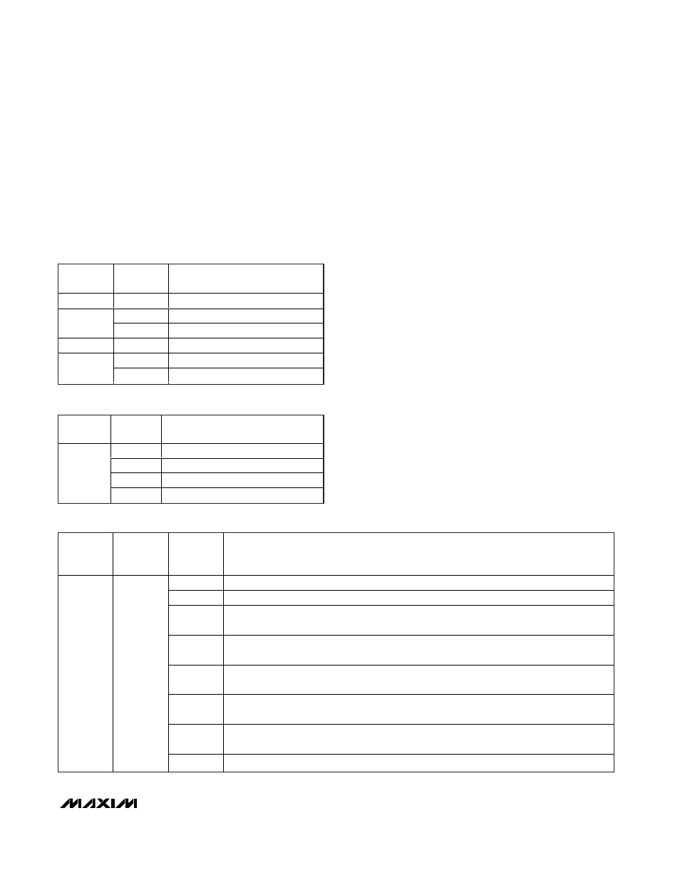
Table 5. ADC Registers for AUXIN1 and
AUXIN2 (Read Only)
REGISTER
ADDRESS
BIT
RANGE
DESCRIPTION
5Ch
[7:0]
AUXIN1 measured value, 8 MSBs.
[1:0]
AUXIN1 measured value, 2 LSBs.
5Dh
[7:2]
Not used.
5Eh
[7:0]
AUXIN2 measured value, 8 MSBs.
[1:0]
AUXIN2 measured value, 2 LSBs.
5Fh
[7:2]
Not used.
Table 6. GPI1–GPI4 Active Logic States
REGISTER
ADDRESS
BIT
RANGE
D ESC R IPT IO N
[0]
G P I1. 0 = acti ve l ow . 1 = acti ve hi g h.
[1]
G P I2. 0 = acti ve l ow . 1 = acti ve hi g h.
[2]
G P I3. 0 = acti ve l ow . 1 = acti ve hi g h.
3Bh
[3]
G P I4. 0 = acti ve l ow . 1 = acti ve hi g h.
Table 7. Programmable Output Behavior and MR
REGISTER
ADDRESS
EEPROM
MEMORY
ADDRESS
BIT
RANGE
DESCRIPTION
[0]
PO1 (MAX6870 only). 0 = PO1 independent of MR. 1 = PO1 asserts when MR = low.
[1]
PO2 (MAX6870 only). 0 = PO2 independent of MR. 1 = PO2 asserts when MR = low.
[2]
PO3 (MAX6870)/PO1 (MAX6871). 0 = PO3/PO1 independent of MR.
1 = PO3/PO1 asserts when MR = low.
[3]
PO4 (MAX6870)/PO2 (MAX6871). 0 = PO4/PO2 independent of MR.
1 = PO4/PO2 asserts when MR = low.
[4]
PO5 (MAX6870)/PO3 (MAX6871). 0 = PO5/PO3 independent of MR.
1 = PO5/PO3 asserts when MR = low.
[5]
PO6 (MAX6870)/PO4 (MAX6871). 0 = PO6/PO4 independent of MR.
1 = PO6/PO4 asserts when MR = low.
[6]
PO7 (MAX6870)/PO5 (MAX6871). 0 = PO7/PO5 independent of MR.
1 = PO7/PO5 asserts when MR = low.
40h
8040h
[7]
PO8 (MAX6870 only). 0 = PO8 independent of MR. 1 = PO8 asserts when MR = low.