Timing characteristics – Rainbow Electronics MAX6871 User Manual
Page 5
MAX6870/MAX6871
EEPROM-Programmable Hex/Quad
Power-Supply Sequencers/Supervisors with ADC
_______________________________________________________________________________________
5
Note 1:
Specifications guaranteed for the stated global conditions. The device also meets the parameters specified when 0 < V
IN1
< +6.5V, and at least one of V
IN3
through V
IN6
is between +2.7V and +5.5V, while the remaining V
IN3
through V
IN6
are
between 0 and +5.5V.
Note 2:
Device may be supplied from any one of IN_, except IN2.
Note 3:
The internal supply voltage, measured at ABP, equals the maximum of IN3 to IN6 if V
IN1
= 0, or equals +5.4V if V
IN1
>
+6.5V. For +4V < V
IN1
< +6.5V and V
IN3
through V
IN6
> +2.7V, the input that powers the device cannot be determined.
Note 4:
100% production tested at T
A
= +25°C and T
A
= +125°C. Specifications at T
A
= -40°C are guaranteed by design.
Note 5:
V
IN_
> 0.3 x ADC range.
Note 6:
Does not include the inaccuracy of the external +1.25V voltage reference.
Note 7:
DNL implicitly guaranteed by design in a sigma-delta converter.
Note 8:
C
BUS
= total capacitance of one bus line in pF. Rise and fall times are measured between 0.1 x V
BUS
and 0.9 x V
BUS
.
Note 9:
Input filters on SDA, SCL, A0, and A1 suppress noise spikes < 50ns.
Note 10: An additional cycle is required when writing to configuration memory for the first time.
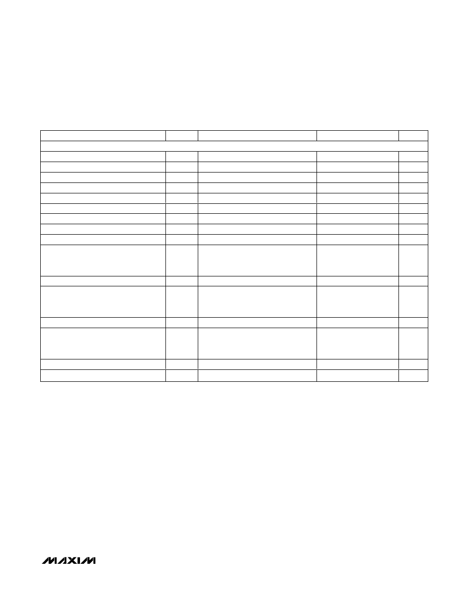
TIMING CHARACTERISTICS
(IN1 = GND, V
IN2
= +10V, V
IN3
to V
IN6
= +2.7V to +5.5V, AUXIN_ = GPI_ = GND, MARGIN = MR = DBP, T
A
= -40°C to +85°C,
unless otherwise noted. Typical values are at T
A
= +25°C.) (Notes 1 and 2)
PARAMETER
SYM B O L
CONDITIONS
MIN
TYP
MAX
UNITS
TIMING CHARACTERISTICS (Figure 2)
Serial Clock Frequency
f
SCL
400
kHz
Clock Low Period
t
LOW
1.3
µs
Clock High Period
t
HIGH
0.6
µs
Bus-Free Time
t
BUF
1.3
µs
START Setup Time
t
SU:STA
0.6
µs
START Hold Time
t
HD:STA
0.6
µs
STOP Setup Time
t
SU:STO
0.6
µs
Data-In Setup Time
t
SU:DAT
100
ns
Data-In Hold Time
t
HD:DAT
0
900
ns
Receive SCL/SDA Minimum Rise Time
t
R
(Note 8)
20 +
0.1 x
C
BUS
ns
Receive SCL/SDA Maximum Rise Time
t
R
(Note 8)
300
ns
Receive SCL/SDA Minimum Fall Time
t
F
(Note 8)
20 +
0.1 x
C
BUS
ns
Receive SCL/SDA Maximum Fall Time
t
F
(Note 8)
300
ns
Transmit SDA Fall Time
t
F
C
BUS
= 400pF
20 +
0.1 x
C
BUS
300
ns
Pulse Width of Spike Suppressed
t
SP
(Note 9)
50
ns
EEPROM Byte Write Cycle Time
t
WR
(Note 10)
11
ms