Timing diagram, Th7887a – Rainbow Electronics TH7887A User Manual
Page 8
8
TH7887A
2146A–IMAGE–05/02
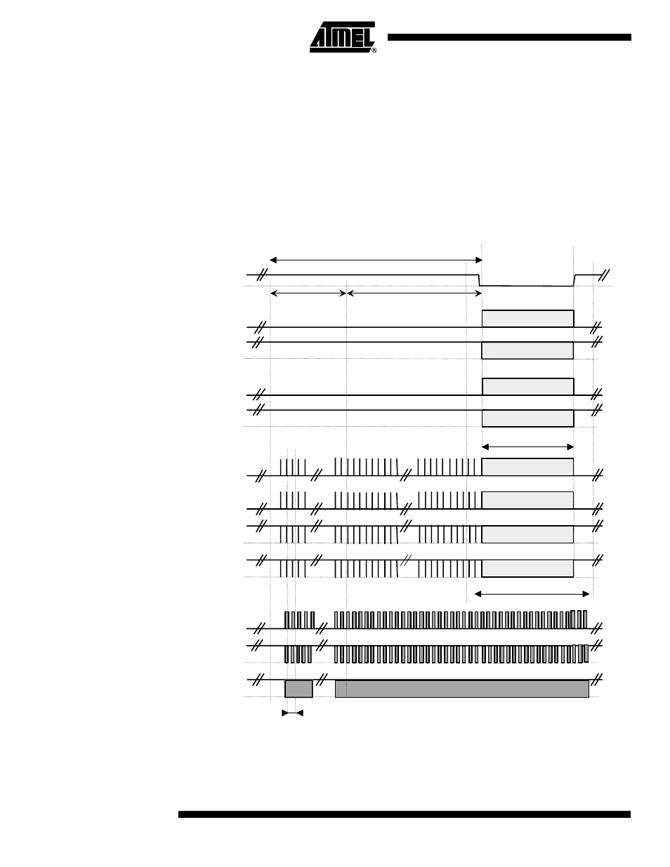
Timing Diagram
The following diagrams are given for:
•
20 MHz readout frequency
•
1.25 MHz vertical transfer frequency
Readout of one image is performed in 2 steps:
•
image zone to memory zone transfer
•
memory zone to register transfer and readout of register
This last step is also an integration period, the duration of which can also be increased
according to the required frame rates.
Figure 5. Frame Timing Diagram
Image to memory zone
Transfer
Picture readout
Integration period
1
5
1044
See fig. 7
See fig. 6
=
Φ
M
1044 pulses
1
5
1044
Memory zone
Cleaning period (*)
(*) During the cleaning period, memory clocks must be pulsed as during readout time
(specially for high temperature applications).
Φ
P1
Φ
M1
Φ
M2
Φ
M3
Φ
M4
Φ
L1
Φ
L2
Φ
R
Φ
A
Φ
P2
Φ
P3
Φ
P4