Th7887a – Rainbow Electronics TH7887A User Manual
Page 10
10
TH7887A
2146A–IMAGE–05/02
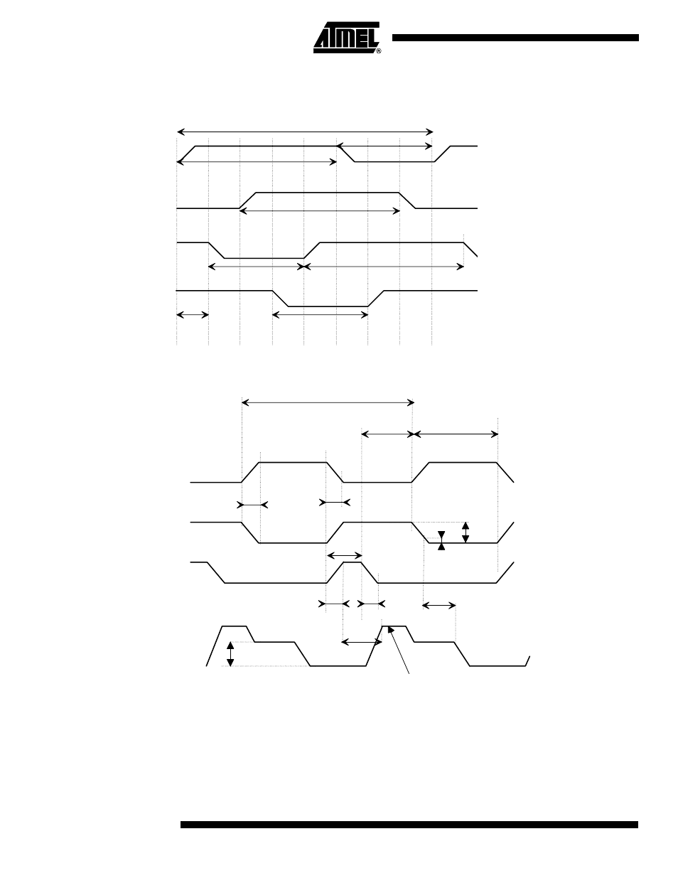
Figure 8. Transfer Period from Image Zone to Memory Zone (
ΦP and ΦM)
for 1.25 MHz Vertical Transfer Frequency (Fv = 1/Tv)
Figure 9. Output Diagram for Readout Register and Reset Clock 20 MHz Applications
Cross over of complementary clocks (
Φ L1, Φ L2) between 30% and 70% of maximum amplitude.
Tv=800 ns
5 To
3 To
5 To
3 To
5 To
To = Tv / 8
3 To
tr
tf
25 ns < tr < To/3
25 ns < tf < To/3
To = 100 ns
=
Φ
M1
Φ
P1
=
Φ
M2
Φ
P2
=
Φ
M3
Φ
P3
=
Φ
M4
Φ
P4
50 ns
t2
t2
t1
12 ns min
t1
16 ns min
16 ns min
Reset feedthrough
t1 = 10 ns typ.
t2 = 5 ns typ.
td = 8 ns typical delay time
Signal
level
td
td
A
0.3A
Φ
L1
Φ
R
Vos 1,2,3,4
Φ
L2