Exposure time reduction, Th7887a – Rainbow Electronics TH7887A User Manual
Page 12
12
TH7887A
2146A–IMAGE–05/02
Exposure Time
Reduction
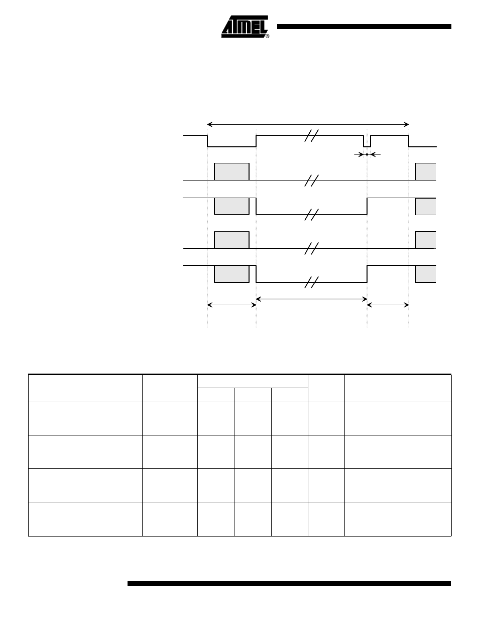
The TH7887A allows exposure time control (electronic shutter function).
The exposure time reduction is achieved by pulsing all the
Φ Pi gates to 0V to continu-
ously remove all photogenerated electrons through antiblooming drain VA.
Figure 12. Timing Diagram for Electronic Shutter
Transfer
Obturation
Integration
Image period
1 µs
1 µs
Fall times and rise times: see figures 7 & 8
Φ
P1
Φ
A
Φ
P2
Φ
P3
Φ
P4
Table 2. Drive Clock Characteristics
Parameter
Symbol
Value
Unit
Remarks
Min
Typ
Max
Image zone clocks
High level
Low level
ΦP1, 2, 3, 4
8.5
0
9
0.5
9.5
0.8
V
V
Typical input capacitance
15 nF
See Figure 13
Memory zone clocks
High level
Low level
ΦM1, 2, 3, 4
8.5
0
9
0.5
9.5
0.8
V
V
Typical input capacitance
15.5 nF
See Figure 13
Memory to register clocks
High level
Low level
ΦM
8.5
0
9
0.5
9.5
0.8
V
V
Typical input capacitance
10 nF
Antiblooming gate
High level (integration)
Low level (transfer)
ΦA
5.5
0
5.5
0.5
5.5
0.8
V
V
Typical input capacitance
14 nF