Rainbow Electronics MAX14514 User Manual
Page 3
MAX14514
Dual Electroluminescent Lamp Driver
_______________________________________________________________________________________
3
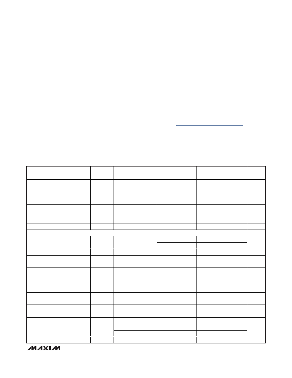
ABSOLUTE MAXIMUM RATINGS
ELECTRICAL CHARACTERISTICS
(V
DD
= +2.7V to +5.5V, C
LAMP_TOTAL
= 10nF, C
CS
= 3.3nF, L
X
= 220µH (I
SAT
= 170mA, R
S
= 5.5
Ω), T
A
= -40°C to +85°C, unless oth-
erwise noted. Typical values are at V
DD
= +3.0V, T
A
= +25°C.) (Note 2)
Stresses beyond those listed under “Absolute Maximum Ratings” may cause permanent damage to the device. These are stress ratings only, and functional
operation of the device at these or any other conditions beyond those indicated in the operational sections of the specifications is not implied. Exposure to
absolute maximum rating conditions for extended periods may affect device reliability.
Note 1: Package thermal resistances were obtained using the method described in JEDEC specification JESD51-7, using a four-layer
board. For detailed information on package thermal considerations, refer to
www.maxim-ic.com/thermal-tutorial
.
(Voltages referenced to GND.)
V
DD
........................................................................-0.3V to +6.0V
CS, LX...................................................................-0.3V to +160V
V
1
, V
2
, COM................................................-0.3V to (V
CS
+ 0.3V)
SW, EL, DIM_, SLEW, CAP, EN ..................-0.3V to (V
DD
+ 0.3V)
Continuous Power Dissipation (T
A
= +70°C)
14-Pin TDFN (derate 24.4mW/°C above +70°C) .......1951mW
Junction-to-Case Thermal Resistance (
θ
JC
) (Note 1)
14-Pin TDFN ...................................................................8°C/W
Junction-to-Ambient Thermal Resistance (
θ
JA
) (Note 1)
14-Pin TDFN .................................................................41°C/W
Operating Temperature Range ...........................-40°C to +85°C
Junction Temperature ......................................................+150°C
Storage Temperature Range .............................-65°C to +150°C
Lead Temperature (soldering, 10s) .................................+300°C
PARAMETER
SYMBOL
CONDITIONS
MIN
TYP
MAX
UNITS
Input Supply Voltage
V
DD
2.7
5.5
V
Input Supply Current
I
IN
R
SLEW
= 375k
Ω, F
EL
= 200Hz,
(V1,V2) - V
COM
= 300V
P-P
700
µA
T
A
= +25°C
40
150
Shutdown Supply Current
I
SHDN
EN = GND
T
A
= - 40°C to + 85°C 400
nA
Shutdown Inductor Supply
Current
I
LX_SHDN
EN = GND, LX = V
DD
, CS = V
DD
1.5
µA
Undervoltage Lockout
V
UV
V
DD
falling
1.8
2.1
2.3
V
Undervoltage Lockout Hysteresis
V
UV_HYST
125
mV
EL OUTPUTS (V
1
, V
2
, COM)
V
DIM_
= +0.5V
105
130
162
V
DIM_
= +1V
210
260
310
Peak-to-Peak Output Voltage
V
_
- V
COM
V
DD
= +3V
V
DIM_
= +1.3V
250
300
350
V
V
1
, V
2
High-Side Switch On-
Resistance
R
ONHS_VN
I
SOURCE
= 1mA
1.5
3.0
k
Ω
V
1
, V
2
Low-Side Switch On-
Resistance
R
ONLS_VN
I
SINK
= 1mA
0.7
2.0
k
Ω
COM High-Side Switch On-
Resistance
R
ON HS _C OM
I
SOURCE
= 1mA
0.7
1.5
k
Ω
COM Low-Side Switch On-
Resistance
R
ON LS _C OM
I
SINK
= 1mA
0.4
1.0
k
Ω
High-Side Switch Off-Leakage
R
ON HS _LEAK
V
1
, V
2
, V
COM
= 0, V
CS
= 150V
-1
+1
µA
Low-Side Switch Off-Leakage
R
ON LS _LE AK
V
1
, V
2
, V
COM
= 150V, V
CS
= 150V
-1
+1
µA
EL Lamp Switching Frequency
f
EL
C
EL
= 872pF, R
SLEW
= 375k
Ω
210
250
290
Hz
Human Body Model
±15
IEC 61000-4-2 Contact Discharge
±4
ESD Protection (COM, V
1
, V
2
Only)
IEC 61000-4-2 Air-Gap Discharge
±4
kV