Detailed description, Input fail-safe, Select function – Rainbow Electronics MAX9393 User Manual
Page 9: Enable function
MAX9392/MAX9393
Anything-to-LVDS Dual 2 x 2
Crosspoint Switches
_______________________________________________________________________________________
9
Detailed Description
The LVDS interface standard provides a signaling
method for point-to-point communication over a con-
trolled-impedance medium as defined by the ANSI
TIA/EIA-644 standard. LVDS utilizes a lower voltage
swing than other communication standards, achieving
higher data rates with reduced power consumption,
while reducing EMI emissions and system susceptibility
to noise.
The MAX9392/MAX9393 1.5GHz dual 2 x 2 crosspoint
switches optimize high-speed, low-power, point-to-
point interfaces. The MAX9392 accepts LVDS and
HSTL signals, while the MAX9393 accepts LVPECL and
CML signals. Both devices route the input signals to
either or both LVDS outputs.
When configured as a 1:2 splitter, the outputs repeat
the selected inputs. This configuration creates copies
of signals for protection switching. When configured as
a repeater, the device operates as a two-channel
buffer. Repeating restores signal amplitude, allowing
isolation of media segments or longer media drive.
When configured as a 2:1 mux, select primary or back-
up signals to provide a protection-switched, fault-toler-
ant application.
Input Fail-Safe
The differential inputs of the MAX9392/MAX9393 pos-
sess internal fail-safe protection. Fail-safe circuitry
forces the outputs to a differential low condition for
undriven inputs or when the common-mode voltage
exceeds the specified range. The MAX9392 provides
high-level input fail-safe detection for LVDS, HSTL, and
other GND-referenced differential inputs. The MAX9393
provides low-level input fail-safe detection for LVPECL,
CML, and other V
CC
-referenced differential inputs.
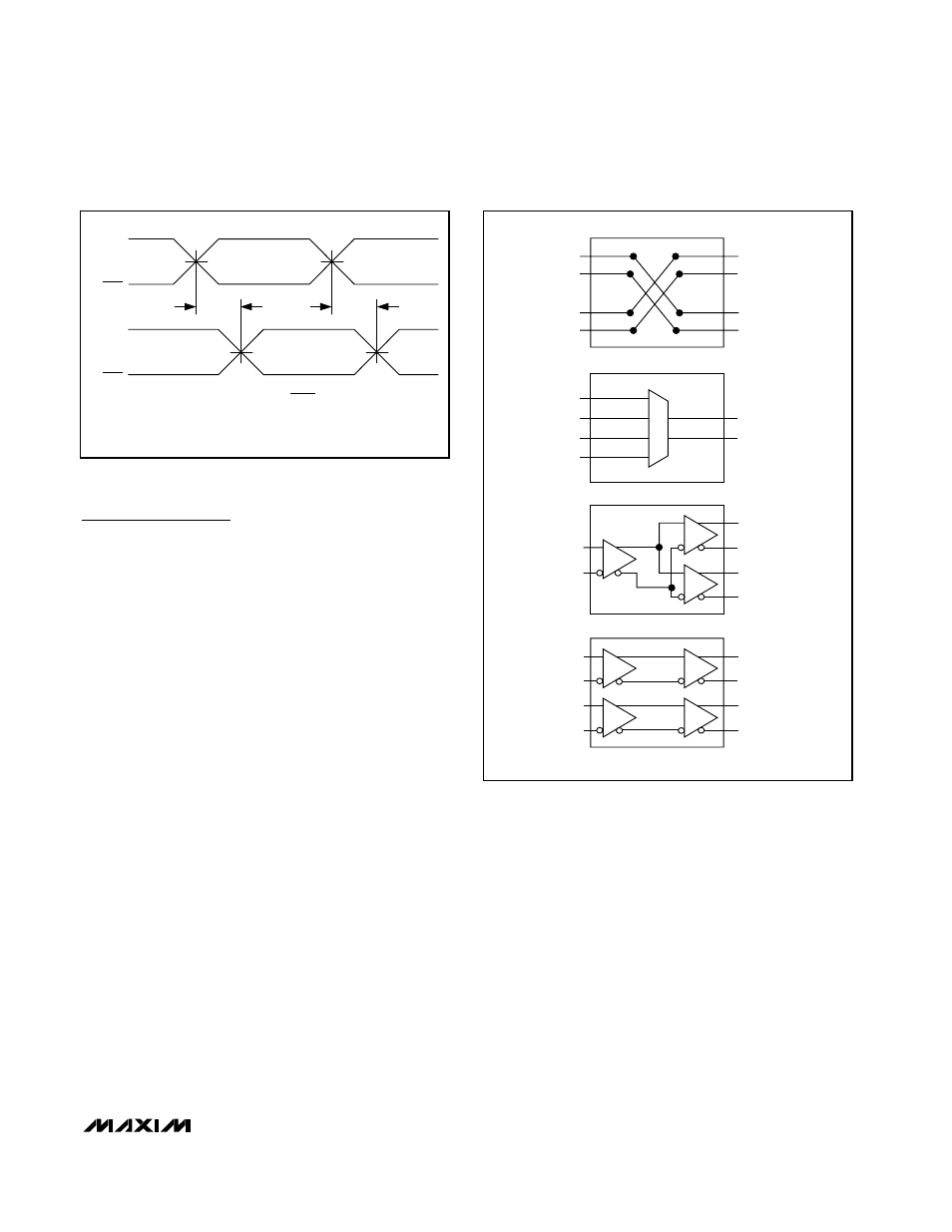
Select Function
The _SEL_ logic inputs control the input and output sig-
nal connections. Two logic inputs control the signal rout-
ing for each channel. _SEL0 and _SEL1 allow the
devices to be configured as a differential crosspoint
switch, 2:1 mux, dual repeater, or 1:2 splitter (Figure 7).
See Table 1 for mode-selection settings (insert A or B for
the _). Channels A and B possess separate select
inputs, allowing different configurations for each channel.
Enable Function
The EN_ _ logic inputs enable and disable each set of
differential outputs. Connect EN_ 0 to V
CC
to enable
the OUT_0/OUT_0 differential output pair. Connect
EN_0 to GND to disable the OUT_0/OUT_0 differential
output pair. The differential output pairs assert to a dif-
ferential low condition when disabled.
V
OD
= V
OUT_ _
- V
OUT_ _
V
OD
= 0
t
CCS
V
OD
= 0
V
OD
= 0
V
OD
= 0
t
CCS
V
OUT_0
V
OUT_0
V
OUT_1
V
OUT_1
t
CCS
MEASURED WITH _SEL0 = _SEL1 = HIGH OR LOW
(1:2 SPLITTER CONFIGURATION).
Figure 6. Output Channel-to-Channel Skew
OUT_0
OUT_0 OR OUT_1
OUT_1
2 x 2 CROSSPOINT
2:1 MUX
1:2 SPLITTER
DUAL REPEATER
OUT_0
OUT_1
OUT_0
OUT_1
IN_0
IN_1
IN_0
IN_1
IN_0
IN_1
IN_0 OR IN_1
Figure 7. Programmable Configurations