Anything-to-lvds dual 2 x 2 crosspoint switches, Applications information, Table 1. input/output function table – Rainbow Electronics MAX9393 User Manual
Page 10
MAX9392/MAX9393
Applications Information
Differential Inputs
The MAX9392/MAX9393 inputs accept any differential
signaling standard within the specified common-mode
voltage range. The fail-safe feature detects common-
mode input signal levels and generates a differential
output low condition for undriven inputs or when the
common-mode voltage exceeds the specified range.
Leave unused inputs unconnected or connect to V
CC
for the MAX9392 or to GND for the MAX9393.
Expanding the Number of LVDS Output
Ports
Cascade devices to make larger switches. Consider
the total propagation delay and total jitter when deter-
mining the maximum allowable switch size.
Power-Supply Bypassing
Bypass each V
CC
to GND with high-frequency surface-
mount ceramic 0.1µF and 0.01µF capacitors in parallel
as close to the device as possible. Install the 0.01µF
capacitor closest to the device.
Differential Traces
Input and output trace characteristics affect the perfor-
mance of the MAX9392/MAX9393. Connect each input
and output to a 50
Ω characteristic impedance trace.
Maintain the distance between differential traces and
eliminate sharp corners to avoid discontinuities in dif-
ferential impedance and maximize common-mode
noise immunity. Minimize the number of vias on the dif-
ferential input and output traces to prevent impedance
discontinuities. Reduce reflections by maintaining the
50
Ω characteristic impedance through connectors and
across cables. Minimize skew by matching the electri-
cal length of the traces.
Output Termination
Terminate LVDS outputs with a 100
Ω resistor between
the differential outputs at the receiver inputs. LVDS out-
puts require 100
Ω termination for proper operation.
Ensure that the output currents do not exceed the cur-
rent limits specified in the Absolute Maximum Ratings.
Observe the total thermal limits of the MAX9392/
MAX9393 under all operating conditions.
Cables and Connectors
Use matched differential impedance for transmission
media. Use cables and connectors with matched differ-
ential impedance to minimize impedance discontinu-
ities. Avoid the use of unbalanced cables. Balanced
cables such as twisted pair offer superior signal quality
and tend to generate less EMI due to canceling effects.
Board Layout
Use a four-layer printed circuit (PC) board providing
separate signal, power, and ground planes for high-
speed signaling applications. Bypass V
CC
to GND as
close to the device as possible. Install termination
resistors as close to receiver inputs as possible. Match
the electrical length of the differential traces to minimize
signal skew.
Anything-to-LVDS Dual 2 x 2
Crosspoint Switches
10
______________________________________________________________________________________
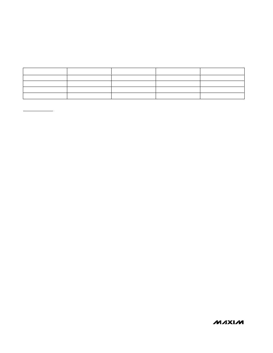
Table 1. Input/Output Function Table
_SEL0
_SEL1
OUT_0 /
OUT_0
OUT_1 /
OUT_1
MODE
0
0
IN_0 / IN_0
IN_0 / IN_0
1:2 splitter
0
1
IN_0 / IN_0
IN_1 / IN_1
Repeater
1
0
IN_1 / IN_1
IN_0 / IN_0
Switch
1
1
IN_1 / IN_1
IN_1 / IN_1
1:2 splitter