Pin description – Rainbow Electronics MAX9393 User Manual
Page 5
MAX9392/MAX9393
Anything-to-LVDS Dual 2 x 2
Crosspoint Switches
_______________________________________________________________________________________
5
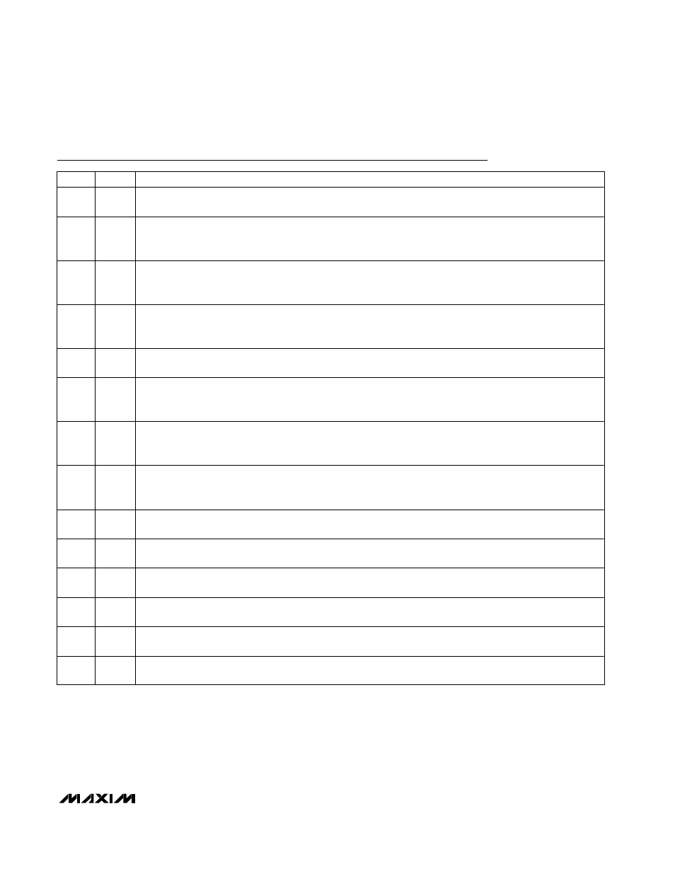
PIN
NAME
FUNCTION
1, 12,
20, 25
GND
Ground
2
INB0
LVDS/HSTL (MAX9392) or LVPECL/CML (MAX9393) Noninverting Input. An internal 128k
Ω resistor to V
CC
pulls
the input high when unconnected (MAX9392). An internal 68k
Ω resistor to GND pulls the input low when
unconnected (MAX9393).
3
INB0
LVDS/HSTL (MAX9392) or LVPECL/CML (MAX9393) Inverting Input. An internal 128k
Ω resistor to V
CC
pulls the
input high when unconnected (MAX9392). An internal 68k
Ω resistor to GND pulls the input low when
unconnected (MAX9393).
4
BSEL0
Input Select for B0 Output. Selects the differential input to reproduce at the B0 differential outputs. Connect
BSEL0 to GND or leave open to select the INB0 (
INB0) set of inputs. Connect BSEL0 to V
CC
to select the INB1
(
INB1) set of inputs. An internal 435k
Ω resistor pulls BSEL0 low when unconnected.
5, 16,
24, 29
V
CC
Power-Supply Input. Bypass each V
CC
to GND with 0.1µF and 0.01µF ceramic capacitors. Install both bypass
capacitors as close to the device as possible, with the 0.01µF capacitor closest to the device.
6
INB1
LVDS/HSTL (MAX9392) or LVPECL/CML (MAX9393) Noninverting Input. An internal 128k
Ω resistor to V
CC
pulls
the input high when unconnected (MAX9392). An internal 68k
Ω resistor to GND pulls the input low when
unconnected (MAX9393).
7
INB1
LVDS/HSTL (MAX9392) or LVPECL/CML (MAX9393) Inverting Input. An internal 128k
Ω resistor to V
CC
pulls the
input high when unconnected (MAX9392). An internal 68k
Ω resistor to GND pulls the input low when
unconnected (MAX9393).
8
BSEL1
Input Select for B1 Output. Selects the differential input to reproduce at the B1 differential outputs. Connect
BSEL1 to GND or leave open to select the INB0 (
INB0) set of inputs. Connect BSEL1 to V
CC
to select the INB1
(
INB1) set of inputs. An internal 435k
Ω resistor pulls BSEL1 low when unconnected.
9
ENB1
B1 Output Enable. Drive ENB1 high to enable the B1 LVDS outputs. An internal 435k
Ω resistor pulls ENB1 low
when unconnected.
10
OUTB1
B1 LVDS Inverting Output. Connect a 100
Ω termination resistor between OUTB1 and OUTB1 at the receiver
inputs to ensure proper operation.
11
OUTB1
B1 LVDS Noninverting Output. Connect a 100
Ω termination resistor between OUTB1 and OUTB1 at the receiver
inputs to ensure proper operation.
13
ENB0
B0 Output Enable. Drive ENB0 high to enable the B0 LVDS outputs. An internal 435k
Ω resistor pulls ENB0 low
when unconnected.
14
OUTB0
B0 LVDS Inverting Output. Connect a 100
Ω termination resistor between OUTB0 and OUTB0 at the receiver
inputs to ensure proper operation.
15
OUTB0
B0 LVDS Noninverting Output. Connect a 100
Ω termination resistor between OUTB0 and OUTB0 at the receiver
inputs to ensure proper operation.
Pin Description