Rainbow Electronics MAX9393 User Manual
Page 2
MAX9392/MAX9393
Anything-to-LVDS Dual 2 x 2
Crosspoint Switches
2
_______________________________________________________________________________________
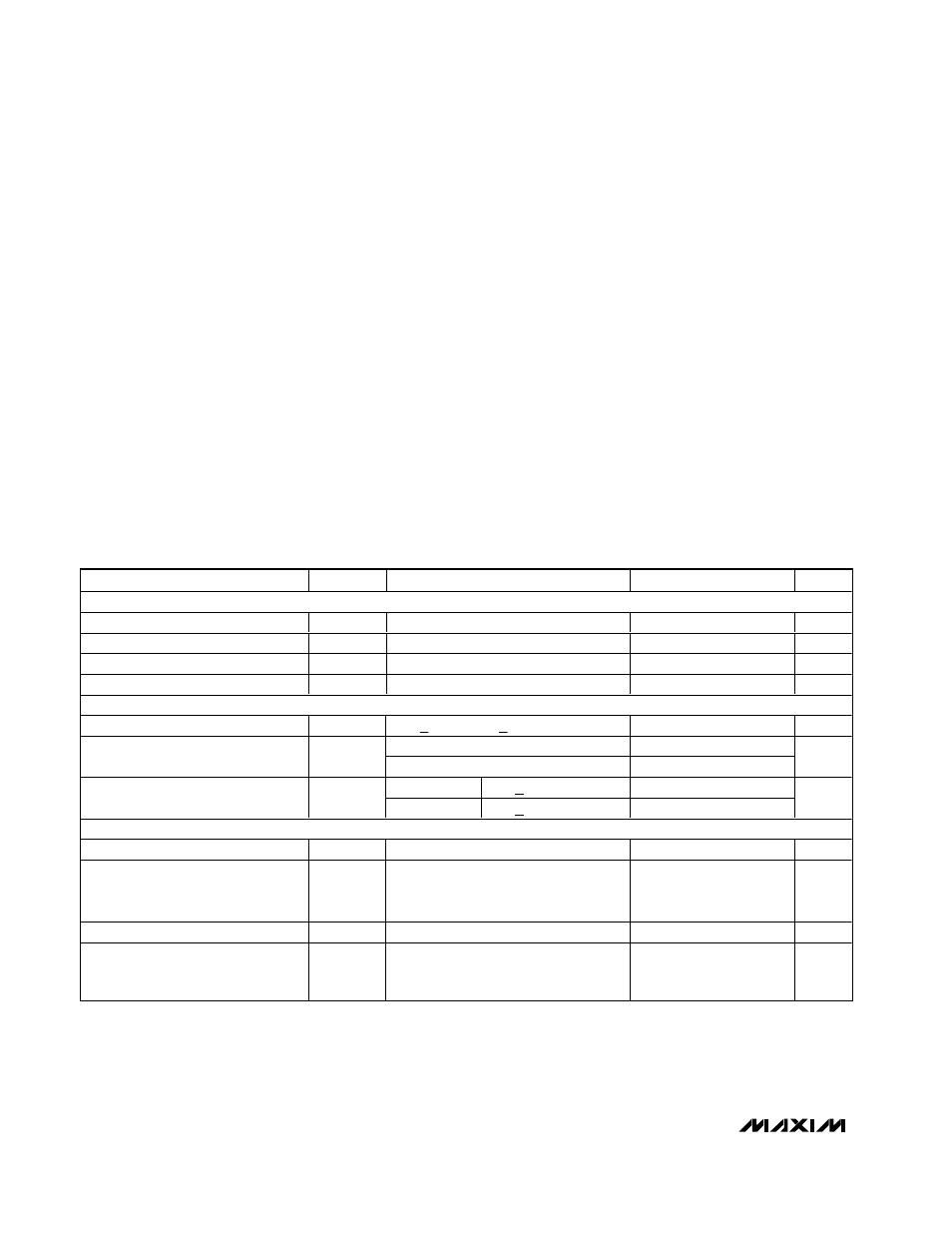
ABSOLUTE MAXIMUM RATINGS
DC ELECTRICAL CHARACTERISTICS
(V
CC
= +3.0V to +3.6V, R
L
= 100
Ω ±1%, EN_ _ = V
CC
, V
CM
= 0.05V to (V
CC
- 0.6V) (MAX9392), V
CM
= 0.6V to (V
CC
- 0.05V)
(MAX9393), T
A
= -40°C to +85°C, unless otherwise noted. Typical values are at V
CC
= +3.3V, |V
ID
| = 0.2V, V
CM
= +1.2V, T
A
= +25°C,
unless otherwise noted.) (Notes 1, 2, and 3)
Stresses beyond those listed under “Absolute Maximum Ratings” may cause permanent damage to the device. These are stress ratings only, and functional
operation of the device at these or any other conditions beyond those indicated in the operational sections of the specifications is not implied. Exposure to
absolute maximum rating conditions for extended periods may affect device reliability.
V
CC
to GND ...........................................................-0.3V to +4.1V
IN_ _, IN_ _, OUT_ _, OUT_ _, EN_ _,
_SEL_ to GND..........................................-0.3V to (V
CC
+ 0.3V)
IN_ _ to IN_ _ ..........................................................................
±3V
Short-Circuit Duration (OUT_ _, OUT_ _) ...................Continuous
Continuous Power Dissipation (T
A
= +70°C)
32-Pin TQFP (derate 13.1mW/°C
above +70°C).............................................................1047mW
32-Pin 5mm x 5mm Thin QFN (derate 21.3mW/°C
above +70°C).............................................................1702mW
Junction-to-Ambient Thermal Resistance in Still Air
32-Pin TQFP............................................................+76.4°C/W
32-Pin 5mm x 5mm Thin QFN....................................+47°C/W
Junction-to-Case Thermal Resistance
32-Pin 5mm x 5mm Thin QFN......................................+2°C/W
Operating Temperature Range ...........................-40°C to +85°C
Junction Temperature ......................................................+150°C
Storage Temperature Range .............................-65°C to +150°C
Soldering Temperature (10s) ...........................................+300°C
PARAMETER
SYM B O L CONDITIONS
MIN
TYP
MAX
UNITS
LVCMOS/LVTTL INPUTS (EN_ _, _SEL_)
Input High Voltage
V
IH
2.0
V
CC
V
Input Low Voltage
V
IL
0
0.8
V
Input High Current
I
IH
V
IN
= +2.0V to V
CC
0
20
µA
Input Low Current
I
IL
V
IN
= 0 to +0.8V
0
10
µA
DIFFERENTIAL INPUTS (IN_ _,
IIIIN
N
N
N__
_
_ __
_
_)
Differential Input Voltage
V
ID
V
ILD
>
0 and V
IHD
<
V
CC
, Figure 1
0.1
3.0
V
MAX9392
0.05
V
CC
- 0.6
Input Common-Mode Range
V
CM
MAX9393
0.6
V
CC
- 0.05
V
MAX9392
|V
ID
|
< 3.0V
-50
+10
Input Current
I
IN_ _
,
I
IN_ _
MAX9393
|V
ID
|
< 3.0V
-10
+90
µA
LVDS OUTPUTS (OUT_ _,
O
O
O
OU
U
U
UT
T
T
T__
_
_ __
_
_)
Differential Output Voltage
V
OD
R
L
= 100
Ω, Figure 2
250
350
450
mV
Change in Magnitude of V
OD
Between Complementary Output
States
∆V
OD
Figure 2
1.0
50
mV
Offset Common-Mode Voltage
V
OS
Figure 2
1.125
1.25
1.375
V
Change in Magnitude of V
OS
Between Complementary Output
States
∆V
OS
Figure 2
1.0
50
mV