Ac electrical characteristics, Dc electrical characteristics (continued) – Rainbow Electronics MAX9393 User Manual
Page 3
MAX9392/MAX9393
Anything-to-LVDS Dual 2 x 2
Crosspoint Switches
_______________________________________________________________________________________
3
AC ELECTRICAL CHARACTERISTICS
(V
CC
= +3.0V to +3.6V, f
IN
< 1.34GHz, t
R_IN
= t
F_IN
= 125ps, R
L
= 100
Ω ±1%, |V
ID
| > 150mV, V
CM
= +0.075V to (V
CC
- 0.6V)
(MAX9392 only), V
CM
= +0.6V to (V
CC
- 0.075V) (MAX9393 only), EN_ _ = V
CC
, T
A
= -40°C to +85°C, unless otherwise noted. Typical
values are at V
CC
= +3.3V, |V
ID
| = 0.2V, V
CM
= +1.2V, f
IN
= 1.34GHz, T
A
= +25°C, unless otherwise noted.) (Note 5)
Note 1: Measurements obtained with the device in thermal equilibrium. All voltages referenced to GND except V
ID
, V
OD
, and
∆V
OD
.
Note 2: Current into the device defined as positive. Current out of the device defined as negative.
Note 3: DC parameters tested at T
A
= +25°C and guaranteed by design and characterization for T
A
= -40°C to +85°C.
Note 4: Current through either output.
Note 5: Guaranteed by design and characterization. Limits set at
±6 sigma.
Note 6: t
SKEW
is the magnitude difference of differential propagation delays for the same output over same conditions. t
SKEW
=
|t
PHL
- t
PLH
|.
Note 7: Measured between outputs of the same device at the signal crossing points for a same-edge transition, under the same
conditions.
Note 8: Device jitter added to the differential input signal.
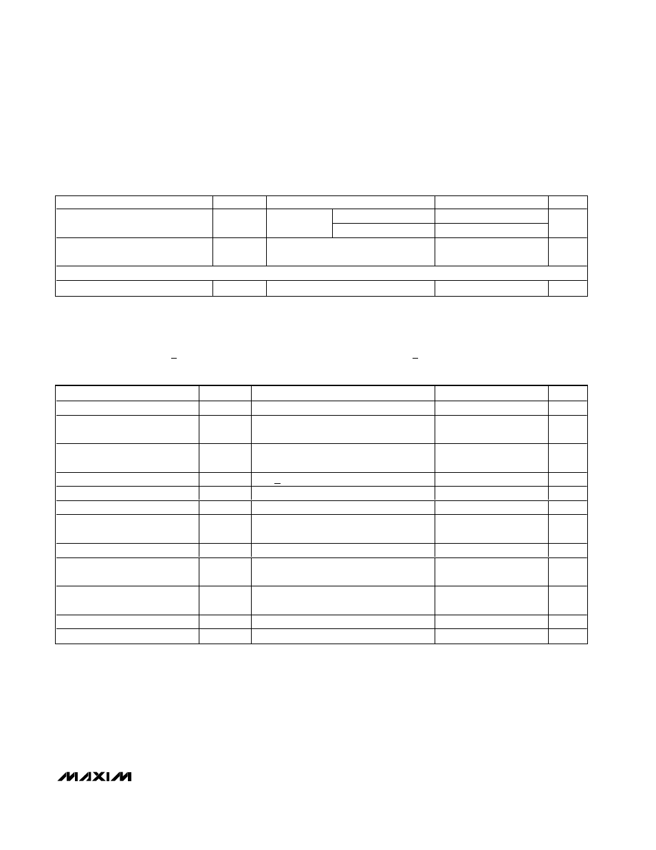
DC ELECTRICAL CHARACTERISTICS (continued)
(V
CC
= +3.0V to +3.6V, R
L
= 100
Ω ±1%, EN_ _ = V
CC
, V
CM
= 0.05V to (V
CC
- 0.6V) (MAX9392), V
CM
= 0.6V to (V
CC
- 0.05V)
(MAX9393), T
A
= -40°C to +85°C, unless otherwise noted. Typical values are at V
CC
= +3.3V, |V
ID
| = 0.2V, V
CM
= +1.2V, T
A
= +25°C,
unless otherwise noted.) (Notes 1, 2, and 3)
PARAMETER
SYM B O L CONDITIONS
MIN
TYP
MAX
UNITS
V
OUT_ _
or V
OUT_ _
= 0
30
40
Output Short-Circuit Current
(Either Output Shorted to GND)
|I
OS
|
V
ID
=
±100m V
( N ote 4)
V
OUT_ _
= V
OUT_ _
= 0
18
24
mA
Output Short-Circuit Current
(Outputs Shorted Together)
|I
OSB
|
V
ID
=
±100mV, V
OUT_ _
= V
OUT_ _
(Note 4)
5.0
12
mA
SUPPLY CURRENT
Supply Current
I
CC
R
L
= 100
Ω, EN_ _ = V
CC
68
98
mA
PARAMETER
SYM B O L CONDITIONS
MIN
TYP
MAX
UNITS
_SEL_ to Switched Output
t
SWITCH
Figure 3
1.1
ns
Disable Time to Differential
Output Low
t
PHD
Figure 4
1.7
ns
Enable Time to Differential
Output High
t
PDH
Figure 4
1.7
ns
Switching Frequency
f
MAX
V
OD
>
250mV
1.5
2.2
GHz
Low-to-High Propagation Delay
t
PLH
Figures 1, 5
294
410
574
ps
High-to-Low Propagation Delay
t
PHL
Figures 1, 5
286
402
555
ps
Pulse Skew |t
PLH
- t
PHL
|
t
SKEW
Figures 1, 5 (Note 6)
17
104
ps
Output-to-Output Skew
t
CCS
Figures 5, 6 (Note 7)
4
67
ps
Output Low-to-High Transition
Time (20% to 80%)
t
R
Figures 1, 5; f
IN
= 100MHz
112
142
185
ps
Output High-to-Low Transition
Time (80% to 20%)
t
F
Figures 1, 5; f
IN
= 100MHz
112
145
185
ps
Added Random Jitter
t
RJ
f
IN_ _
= 1.34GHz, clock pattern (Note 8)
2
ps
RMS
Added Deterministic Jitter
t
DJ
1.34Gbps, 2
23
- 1 PRBS (Note 8)
60
98
ps
P-P