Applications information – Rainbow Electronics MAX5661 User Manual
Page 34
MAX5661
Single 16-Bit DAC with Current and Voltage
Outputs for Industrial Analog Output Modules
34
_______________________________________________________________________________________
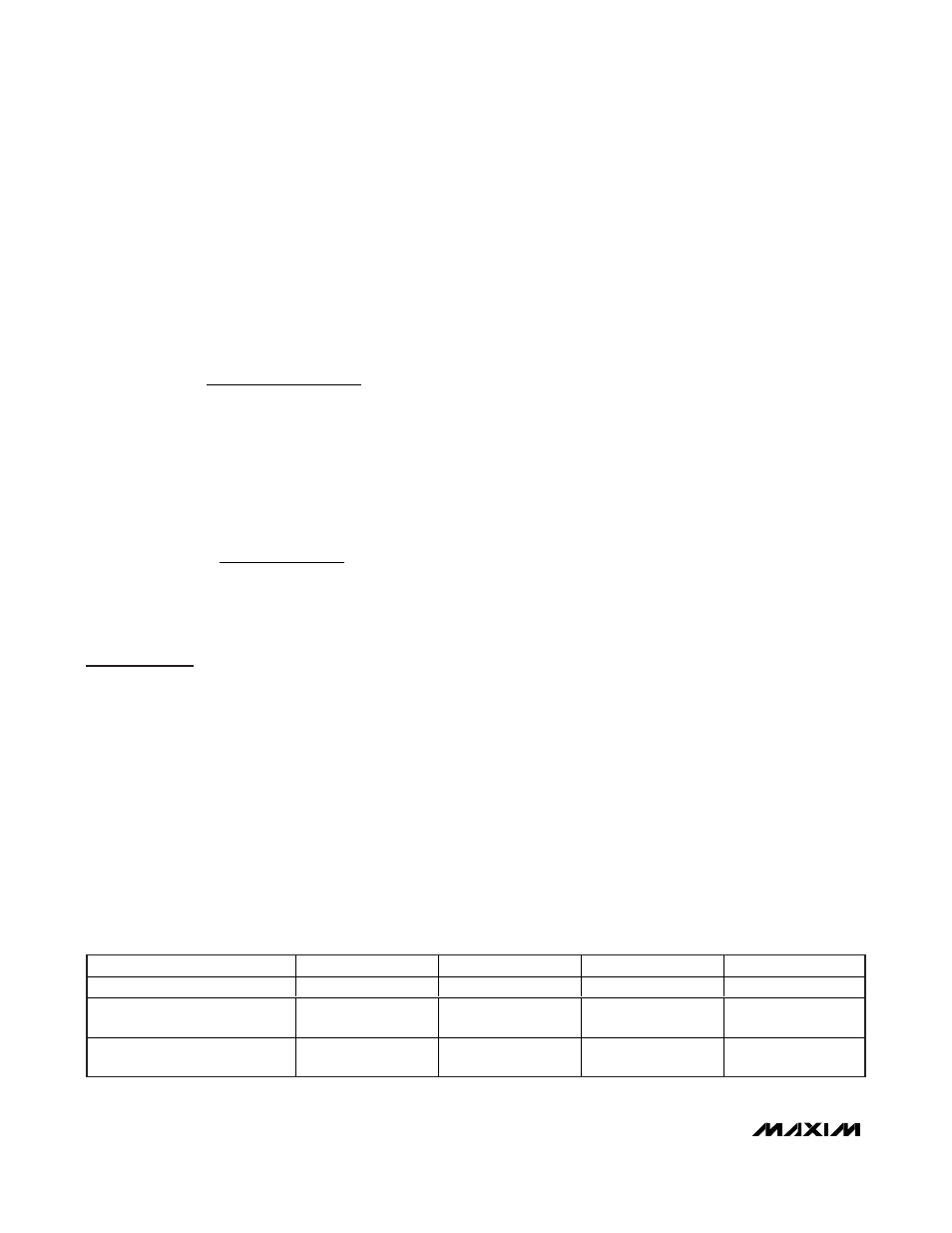
APPLICATION MODE
V
DDV
V
SSV
V
DDI
V
DDCORE
Voltage from OUTV
+13.48V to +15.75V
-13.48V to -15.75V
V
DDV
V
DDV
Current from OUTI
(Single Supply)
AGND
AGND
+13.48V to +40V
V
DDI
Voltage from OUTV and Current
from OUTI*
+13.48V to +15.75V
-13.48V to -15.75V
V
DDV
to +40V
V
DDV
Table 16. Application Modes and Supply-Voltage Limits
*
On-the-fly switching. Only one output is active at a time.
Measuring Zero-Code Current
(0 to 20mA Mode)
After setting the MAX5661 for 0 to 20mA current-range
mode, determine the LSB size as follows:
1) Measure I
OUT
at full scale (FS).
2) Measure I
OUT
at code 192.
3) Measure I
OUT
at code 193:
If I
OUT
(code 193) - I
OUT
(code 192) > 0.5 I
LSB
, I
OUT
(code 192) is inside the linear region of the I
OUT
trans-
fer curve.
Obtain the straight-line equation from I
OUT
(FS) and
I
OUT
(192) and substituting code 0 for I
OUT
(zero scale)
in the equation:
The expected current is -30µA (typ).
Applications Information
Power-Supply Sequencing and Bypassing
After connecting all ground inputs, apply the analog
supply voltages V
SSV
first followed by the most positive
supply, the second most positive supply, etc. Before
applying power, connect the V
DDCORE
supply to either
V
DDV
or V
DDI
, as shown in Table 16, depending on
whether the current output or voltage output is used. Do
not apply V
DDCORE
separate from the main supply
(V
DDV
/V
SSV
or V
DDI
) in the preferred configuration
(Table 16). Ensure that there are no unconnected
power-supply connections when powering the
MAX5661. If V
SSV
cannot be powered first, connect a
Schottky diode between V
SSV
and AGND.
Daisy Chaining Multiple MAX5661 Devices
In standard SPI-/QSPI-/MICROWIRE-compatible sys-
tems, a microcontroller (µC) communicates with its
slave devices through a 3- or 4-wire serial interface.
The typical interface includes a chip select signal (CS),
a serial clock (SCLK), a data input signal (DIN), and
sometimes a data signal output (DOUT). In this system,
the µC allots an independent chip-select signal to each
slave device so that they can be addressed individually
(see Figure 10). Only the slaves with their CS inputs
asserted low acknowledge and respond to the activity
on the serial clock and data lines. This is simple to
implement when there are very few slave devices in the
system. An alternative programming method is daisy
chaining. Daisy chaining, in serial-interface applica-
tions, is a method of propagating commands through
multiple devices connected in series (see Figure 11).
Daisy chaining reduces CS and DIN line routing, and
saves board space when using the MAX5661.
Daisy chain multiple MAX5661 devices by connecting
the DOUT of one device to the DIN of the next. Connect
the SCLK of all devices to a common clock and connect
the CS from all devices to a common chip-select line.
Data shifts out of DOUT 24.5 clock cycles after it is shift-
ed into DIN on the falling edge of SCLK. Hold CS low
until each slave in the chain receives its 24-bit word (8
command bits and 16 data bits). In this configuration,
the µC only needs three signals (CS, SCLK, and DIN) to
control all the slaves in the network. The SPI-/QSPI-
/MICROWIRE-compatible serial interface normally works
at up to 10MHz, but must be slowed to 6MHz if daisy
chaining. DOUT is high impedance when CS is high.
Figure 10 details a method of controlling multiple
MAX5661 devices using separate CS lines. This
method allows writes to and reads from each device
without shifting data through the other device’s shift
register. Figure 10 shows the FAULT outputs shorted
together. This configuration requires a read from each
device to determine which one has the fault condition
and saves an optocoupler in isolated applications. It is
not necessary to short the FAULT outputs together.
(
)
I I
at
I
at FS I
OUT
OUT
OUT
−
=
−
192
a
at
x code
I
OUT
(
)
192
65535 192
192
−
⎛
⎝
⎜
⎞
⎠
⎟
−
(
)
.
at ZS
I
at
I
at FS x
OUT
OUT
=
−
192
0 002
29383
192
+ I
at
OUT
I
LSB
I
at FS
I
at
OUT
OUT
(
)
=
−
−
−
192
2
1
192
16