Pin description (continued) – Rainbow Electronics MAX5661 User Manual
Page 18
MAX5661
Single 16-Bit DAC with Current and Voltage
Outputs for Industrial Analog Output Modules
18
_______________________________________________________________________________________
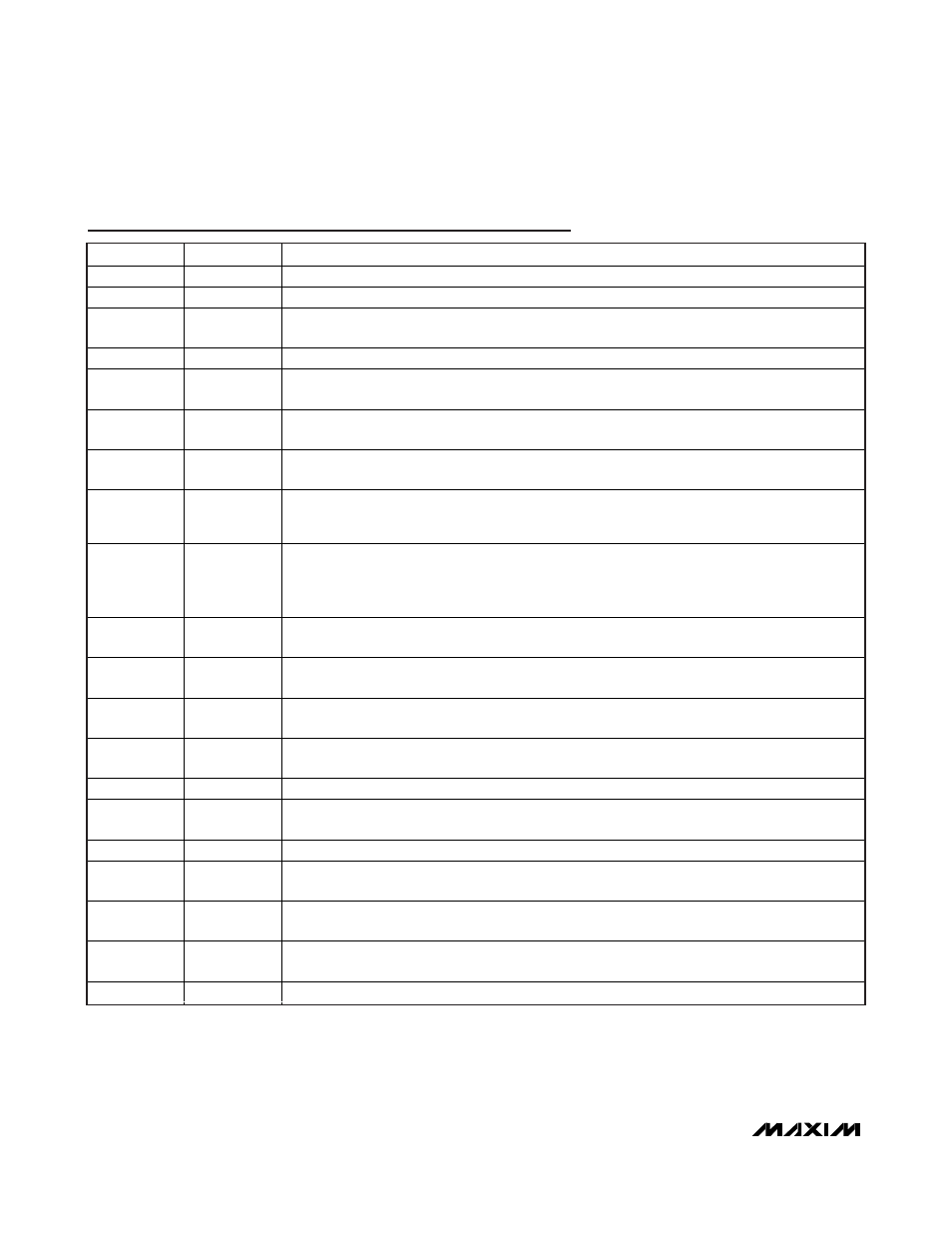
Pin Description (continued)
PIN
NAME
FUNCTION
22
DIN
Serial-Data Input. Data is clocked into the serial interface on the rising edge of SCLK.
23
SCLK
Serial-Clock Input
24
CS
Active-Low Chip-Select Input. Drive CS low to enable the serial interface. Drive CS high to disable
the serial interface. DOUT is high impedance when CS is high.
25
DGND
Digital Ground
26
VCC
Digital Power Supply. Connect V
CC
to a power supply between +4.75V and +5.25V. Bypass V
CC
with a 0.1µF capacitor to DGND, as close as possible to the device.
27
LDAC
Active-Low Asynchronous Load DAC Input. Drive LDAC low to transfer the contents of the input
register to the DAC register to immediately update the output. Connect LDAC to V
CC
if unused.
28
FAULT
Active-Low Open-Drain Fault Output. FAULT asserts low for an OUTI open-circuit condition, an
OUTV short-circuit condition, or when the CLR input is low (see Table 12 and Figure 9).
35
DOUT
Serial Data Output. Data transitions at DOUT on SCLK’s falling edge. DOUT is high impedance
when CS is high. Use DOUT to read the shift register contents or for daisy chaining multiple
MAX5661 devices.
37
CLR
Active-Low Clear Input. Drive CLR low to set the DAC code to the value stored in the clear
register, to 0V in voltage mode, or 0mA/4mA depending on the output current mode. Program the
contents of the clear register through the serial interface. Enable and disable the CLR input
through the control register’s CLREN bit (see Table 4).
39
VDDCORE
DAC Core Positive Supply. Connect V
DDCORE
to V
DDI
or V
DDV
(see Table 16). Bypass V
DDCORE
with a 0.1µF capacitor to AGND, as close as possible to the device.
40
DUTGNDS
DUT Analog Sense Ground. Connect DACGND, DACGNDS, DUTGND, and DUTGNDS together
on a low-noise ground plane with a star connection.
41
DUTGND
DUT Analog Ground. Connect DACGND, DACGNDS, DUTGND, and DUTGNDS together on a
low-noise ground plane with a star connection.
43
COMPV
OUTV Amplifier Compensation Feedback Node. Connect a 3.3nF capacitor from OUTV to COMPV
when OUTV drives capacitive loads of up to 1.2µF. Leave COMPV open for faster response time.
45
AGND
Analog Ground
53
SVP
Remote Ground Sense Input. Connect SVP to the bottom terminal of R
OUTV
. See the Typical
Operating Circuit.
54, 59
I.C.
Internal Connection. Leave unconnected.
55
VSSV
D AC V ol tag e- Outp ut N eg ati ve P ow er S up p l y. Al w ays connect V
S S V
to a p ow er sup p l y b etw een - 13.48V
and -15.75V. Bypass V
SSV
with a 0.1µF capacitor to AGND, as close as possible to the device.
56
OUTV
DAC Unipolar/Bipolar Voltage Output. OUTV provides 0 to +10.48V in unipolar mode and -10.48V
to +10.48V in bipolar mode.
57
VDDV
DAC Voltage-Output Positive Power Supply. Connect V
DDV
to a power supply between +13.48V
and +15.75V. Bypass V
DDV
with a 0.1µF capacitor to AGND, as close as possible to the device.
60
SVN
Rem ote V ol tag e S ense Inp ut. C onnect to the top ter m i nal of R
OU T V
. S ee the Typ i cal Op er ati ng C i r cui t.