Table 14. cnf1/cnf0 hardware settings – Rainbow Electronics MAX5661 User Manual
Page 31
MAX5661
Single 16-Bit DAC with Current and Voltage
Outputs for Industrial Analog Output Modules
______________________________________________________________________________________
31
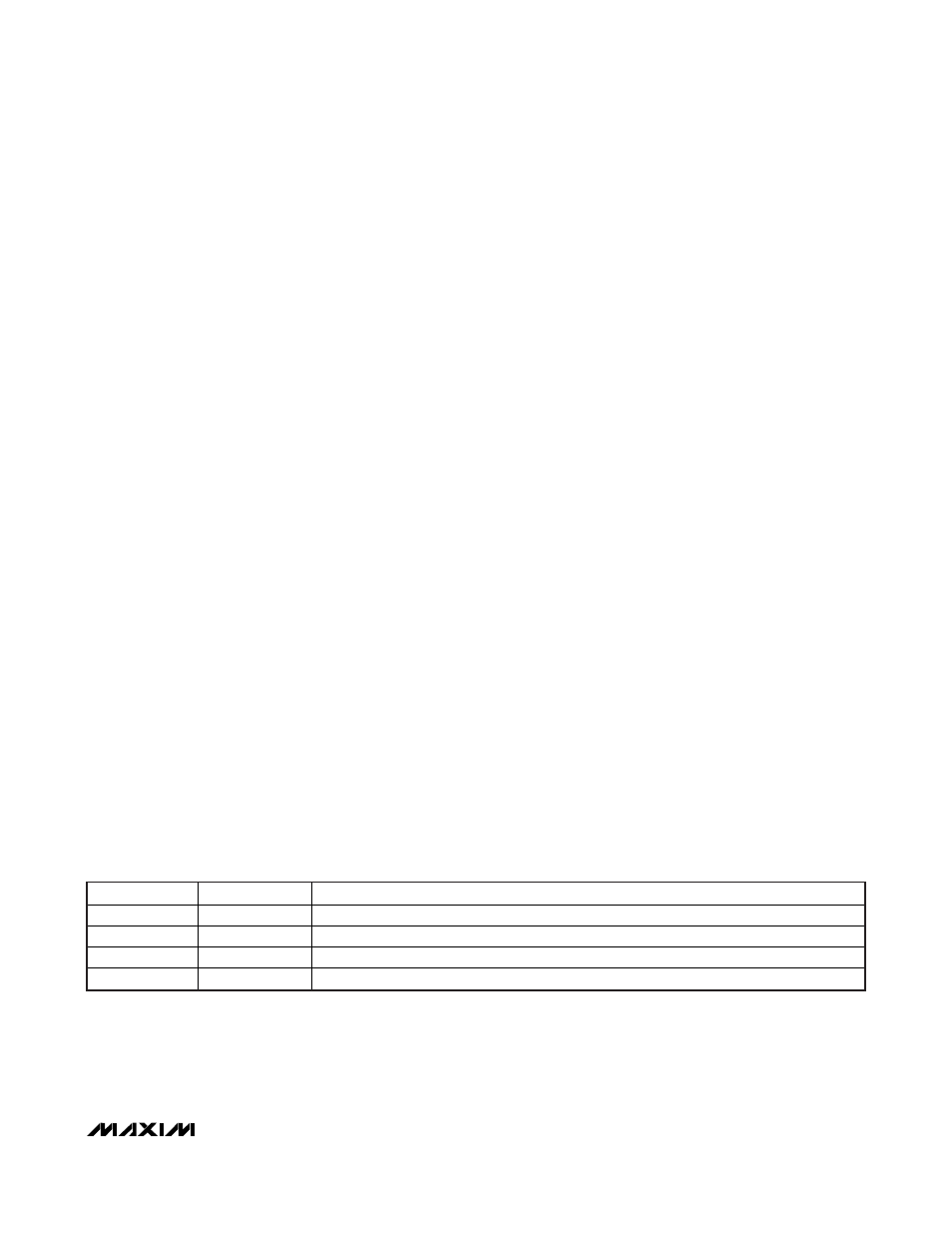
CNF0/CNF1 Hardware Inputs
The CNF0 and CNF1 inputs enable the DAC’s voltage
(OUTV) or current (OUTI) outputs. Drive CNF0 and
CNF1 low to disable both the OUTV and OUTI outputs.
Drive CNF0 high and CNF1 low to enable the OUTI out-
put. Drive CNF0 low and CNF1 high to enable the
OUTV output. Drive CNF0 and CNF1 high to control the
OUTV and OUTI outputs through the serial interface.
Table 14 summarizes the output behavior when pro-
grammed by the CNF0/CNF1 hardware inputs.
OUTI Current-Output Configuration
Drive CNF0 high and CNF1 low to enable the OUTI out-
put through the hardware. Alternatively, drive CNF0 and
CNF1 high to control OUTI with the serial interface. With
CNF1 and CNF0 high, the control register’s
OUTION bit enables the OUTI output. Set OUTION to 1
to enable the OUTI output. Set OUTION to 0 (default
power-up state) to disable the OUTI output.
The OUTI current output derives power from V
DDI
and
V
DDCORE
(+13.48V to +40V). Connect V
DDCORE
to
V
DDI
when using the OUTI output.
The control register’s OUTI4/0EN bit (see Tables 4 and
13) determines whether the OUTI4/0 hardware input or
the control register’s I4TO20BIT bit controls the OUTI
current range. Set the OUTI4/0EN bit to 0 (default
power-up state) to control the current range through the
OUTI4/0 hardware input. Connect the OUTI4/0 hard-
ware input to AGND to select the 0 to 20mA mode.
Connect the OUTI4/0 hardware input to V
DDI
to select
the 4–20mA mode.
Set the OUTI4/0EN bit to 1 to allow software control of
the OUTI current range through the I4TO20BIT bit (see
Table 13). Set I4TO20BIT to 0 to select the 0 to 20mA
mode. Set I4TO20BIT to 1 to select the 4–20mA mode.
OUTV Voltage-Output Configuration
Drive CNF0 low and CNF1 high to enable the OUTV
output through the hardware (see Table 14).
Alternatively, drive CNF0 and CNF1 high to control
OUTV with the serial interface. With CNF1 and CNF0
high, the control register’s OUTVON bit enables the
OUTV output. Set OUTVON to 1 to enable the OUTV
output. Set OUTVON to 0 (default power-up state) to
disable the OUTV output.
The OUTV output derives power from V
DDV
, V
SSV
, and
V
DDCORE
. Connect V
DDCORE
to V
DDV
(+13.48V to
+15.75V) when using the OUTV output. Always connect
a negative supply to V
SSV
(-13.48V to -15.75V) (see
Table 16).
The control register’s B/U bit sets OUTV for bipolar or
unipolar mode. Set B/U to 0 (default power-up state) to
select the bipolar output range (±10.48V). Set B/U to 1
to select the unipolar output range (0 to +10.48V).
Output Transfer Functions
The DAC output voltage/current is a function of the vari-
ous hardware control inputs and digital inputs in the
control register (see Table 13). The transfer functions
below assume that the outputs are on, and a reference
voltage of +4.096V is applied to the reference input. For
the voltage output, the sense input is at the same
potential as the DAC output (OUTV = SVP and AGND =
SVN). Table 15a details the bipolar output voltage
transfer function. Table 15b details the unipolar output
voltage transfer function. Table 15c details the 0 to
20mA current-range transfer function. Table 15d details
the 4mA to 20mA current-range transfer function.
CNF1
CNF0
OUTV, OUTI SETTING
DGND
DGND
Both DAC outputs disabled.
DGND
V
CC
OUTI enabled. OUTV disabled.
V
CC
DGND
OUTV enabled. OUTI disabled.
V
CC
V
CC
DAC outputs controlled by the serial interface.
Table 14. CNF1/CNF0 Hardware Settings