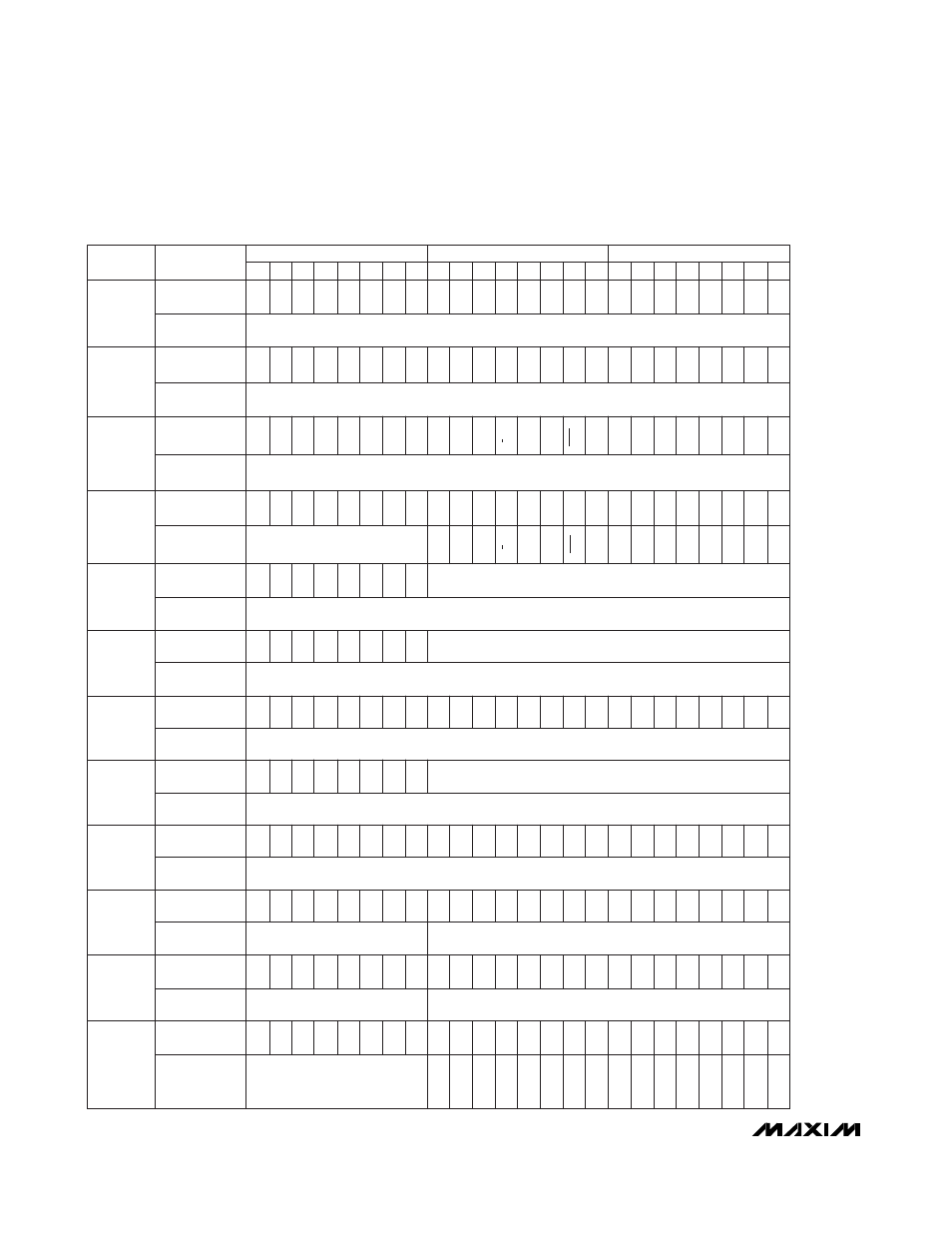
Table 3. register bit descriptions – Rainbow Electronics MAX5661 User Manual
Page 22
MAX5661
Single 16-Bit DAC with Current and Voltage
Outputs for Industrial Analog Output Modules
22
_______________________________________________________________________________________
OPERATION
No operation.
Transfer shift-
register data
to DOUT.
No operation.
Transfer shift-
register data
to DOUT.
COMMAND BYTE
1ST DATA BYTE
2ND DATA BYTE
C7
C6
C5
C4
C3
C2
C1
C0
D15
D14
D13
D12
D11
D10
D9
D8
D7
D6
D5
D4
D3
D2
D1
D0
Write control
register
Read control
register
X
X
X
X
X
X
X
X
X
X
X
X
0
0
0
0
1
1
1
1
0
0
0
1
0
X
X
X
X
X
X
X
X
X
X
X
X
X
X
X
X
X
X
X
X
X
X
X
X
X
X
X
X
X
X
X
X
X
X
X
X
X
Same as line above. Shift-register data not changed by this operation.
Same as line above. Shift-register data not changed by this operation.
Same as line above. Shift-register data not changed by this operation.
X
X
X
X
0
0
1
0
X
X
X
X
X
X
X
Same as line above.
X
X
X
X
X
X
X
X
X
X
X
Load input
register from shift
register. DAC
register unchanged.
X
X
X
X
0
0
1
1
MSB <-- 16-Bit DAC Data --> LSB
Same as line above. Shift-register data not changed by this operation.
Load input
register and DAC
register from shift
register.
X
X
X
X
0
1
0
0
MSB <-- 16-Bit DAC Data --> LSB
Same as line above. Shift-register data not changed by this operation.
Load DAC register
from input
register
X
X
X
X
0
1
0
1
X
X
X
X
X
X
X
X
X
X
X
X
X
X
X
X
Same as line above. Shift-register data not changed by this operation.
Write clear
register
X
X
X
X
0
1
1
0
MSB <-- 16-Bit Clear-Register Data --> LSB
Same as line above. Shift-register data not changed by this operation.
Read input register
Read DAC
register
Read clear
register
Data in shift register
after
CS driven high and
command executed
Data in shift register
after
CS driven high and
command executed
Data in shift register
after
CS driven high and
command executed
Data in shift register
after
CS driven high and
command executed
Data in shift register
after
CS driven high and
command executed
Data in shift register
after
CS driven high and
command executed
Data in shift register
after
CS driven high and
command executed
Data in shift register
after
CS driven high and
command executed
Data in shift register
after
CS driven high and
command executed
Data in shift register
after
CS driven high and
command executed
Data in shift register
after
CS driven high and
command executed
Data in shift register
before
CS driven high and
command executed
Data in shift register
before
CS driven high and
command executed
Data in shift register
before
CS driven high and
command executed
Data in shift register
before
CS driven high and
command executed
Data in shift register
before
CS driven high and
command executed
Data in shift register
before
CS driven high and
command executed
Data in shift register
before
CS driven high and
command executed
Data in shift register
before
CS driven high and
command executed
Data in shift register
before
CS driven high and
command executed
Data in shift register
before
CS driven high and
command executed
Data in shift register
before
CS driven high and
command executed
X
X
X
X
0
1
1
1
X
X
X
X
X
X
X
X
X
X
X
X
X
X
X
X
X
X
X
X
1
0
0
0
X
X
X
X
X
X
X
X
X
X
X
X
X
X
X
X
X
X
X
X
1
0
0
1
X
X
X
X
X
X
X
X
X
X
X
X
X
X
X
X
Same as line above.
Same as line above.
Same as line above.
MSB <-- 16-Bit Input-Register Data --> LSB
MSB <-- 16-Bit DAC-Register Data --> LSB
MSB <-- 16-Bit DAC Clear Register Data --> LSB
Write full-scale
output trim
register
Data in shift register
after
CS driven high and
command executed
Data in shift register
before
CS driven high and
command executed
X
X
X
X
1
0
1
0
1
X
X
X
X
X
X
X
X
X
X
X
X
X
X
X
X
X
X
X
X
Same as line above.
0
OUTVON
OUTVON
OUTION
OUTION
CLREN
CLREN
FAUL
TEN
FAUL
TEN
FAUL
TV
FAUL
TI
RCLR
RCLR
CLRMODE
CLRMODE
CLRFLAGEN
CLRFLAGEN
CLEARST
14 to 20 BIT
14 to
20 BIT
OUTI4/
0
EN
OUTI4/
0
EN
B/U
B/U
FS_ EN
FS_ BIT 9 (MSB)
FS_ BIT 0 (LSB)
FS_ BIT 6
FS_ BIT 4
FS_ BIT 3
FS_ BIT 7
FS_ BIT 8
FS_ BIT 5
FS_ BIT 2
FS_ BIT 1
DESCRIPTION
Table 3. Register Bit Descriptions