Rainbow Electronics MAX5661 User Manual
Page 2
MAX5661
Single 16-Bit DAC with Current and Voltage
Outputs for Industrial Analog Output Modules
2
________________________________________________________________________________________
V
DDCORE
to V
SSV
...................................................-0.3V to +42V
V
DDI
to AGND.........................................................-0.3V to +42V
V
DDV
to AGND........................................................-0.3V to +17V
V
SSV
to AGND ........................................................-17V to +0.3V
V
DDI
to V
SSV
...........................................................-0.3V to +59V
V
CC
to DGND ...........................................................-0.3V to +6V
DGND, DUTGND, DUTGNDS, DACGND,
DACGNDS to AGND ............................................-0.3V to +6V
Digital Inputs (CS, DIN, SCLK, CLR, LDAC,
CNF_) to DGND .....................................-0.3V to (V
CC
+ 0.3V)
Digital Outputs (DOUT, FAULT) to DGND....................................
...............................-0.3V to the lesser of (V
CC
+ 0.3V) or +6V
REF to AGND............................................................-0.3V to +6V
OUTV, SVP, SVN, COMPV to V
SSV
...........-0.3V to (V
DDV
+ 0.3V)
OUTI, COMPI, OUTI4/0 to AGND ..............-0.3V to (V
DDI
+ 0.3V)
Maximum Current into Any Pin .......................................±100mA
Continuous Power Dissipation (T
A
= +70°C)
64-Pin, 10mm x 10mm TQFP (derate 25mW/°C
above +70°C)............................................................ 2000mW
Junction-to-Ambient Thermal Resistance
in Still Air (θ
JA
) ...………………………………………….40°C/W
Junction-to-Case Thermal Resistance (θ
JC
)...................... 8°C/W
Operating Temperature Range .........................-40°C to +105°C
Junction Temperature ......................................................+150°C
Storage Temperature Range .............................-65°C to +150°C
Lead Temperature (soldering,10s) ..................................+300°C
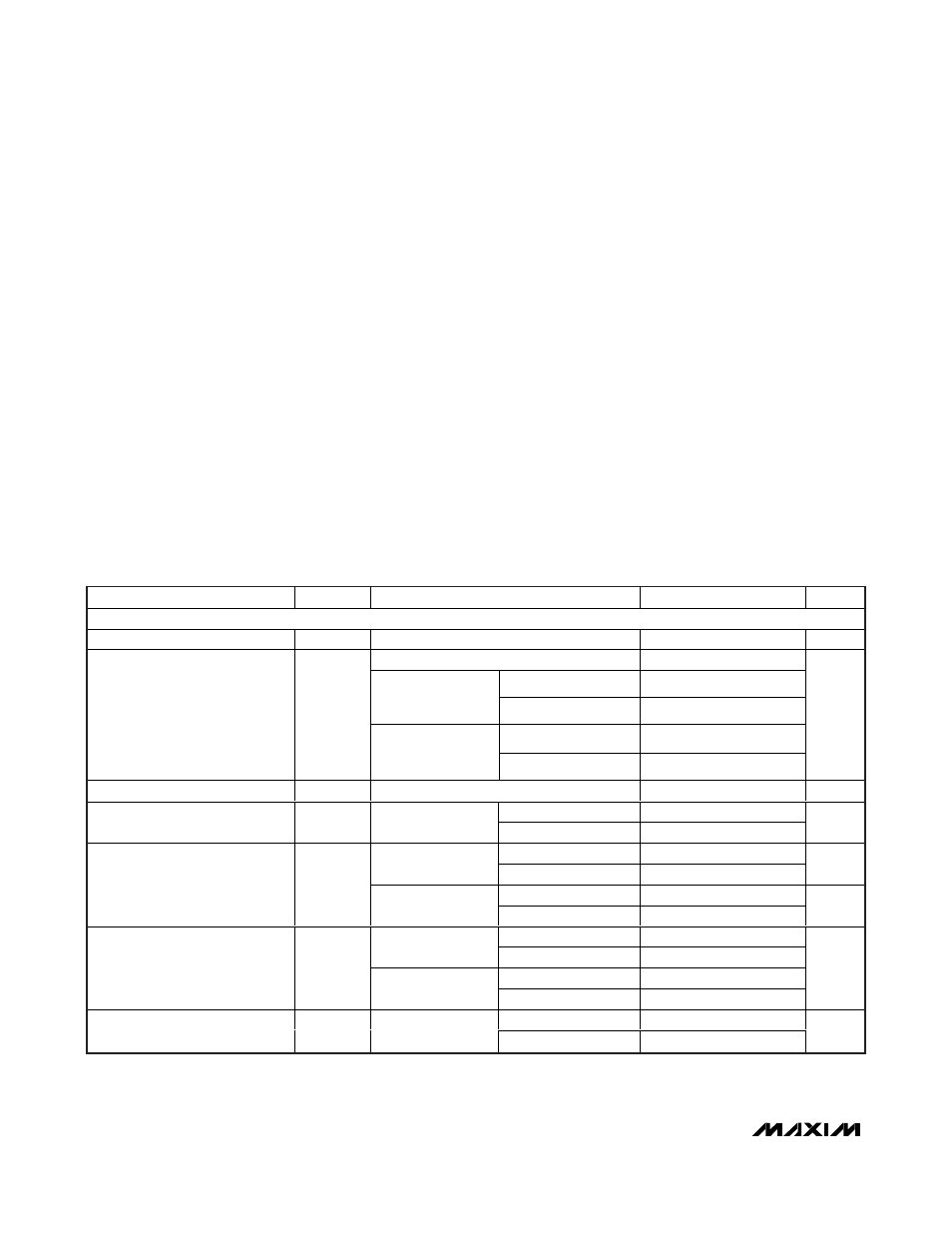
ABSOLUTE MAXIMUM RATINGS
ELECTRICAL CHARACTERISTICS
(V
CC
= +5V, C
COMPI
= 22nF, V
DDV
= V
DDCORE
= +15V, V
SSV
= -15V, V
DDI
= +24V, V
REF
= +4.096V, V
AGND
= V
DGND
= V
DUTGND
=
V
DACGND
= 0V, R
SERIES
= 47Ω, OUTV loaded with 2kΩ || 100pF to AGND, OUTI loaded with 500Ω to AGND, T
A
= -40°C to +105°C,
unless otherwise noted. Typical values are at T
A
= +25°C. See the
Typical Operating Circuit.) (Note 1)
PARAMETER
SYM B O L CONDITIONS
MIN
TYP
MAX
UNITS
STATIC PERFORMANCE
Resolution
16
Bits
V
OUT
±0.2
±4
4–20mA
±6
I
OUT
, V
DDI
= 40V,
V
SSV
= V
DDV
= 0
(Note 2)
0 to 20mA
±10
4–20mA
±2
Integral Nonlinearity
INL
I
OUT
, V
DDI
= V
DDV
= + 15V , V
S S V
= - 15V
(Note 2)
0 to 20mA
±6
LSB
Differential Nonlinearity
DNL
Guaranteed monotonic (Note 3)
-1.0
+1.0
LSB
Unipolar
±0.01
±3
Zero-Scale Voltage Error
V
ZSE
OUTV
Bipolar
±2.0
±10
mV
T
A
= +25°C
-45
-30
-15
0 to 20mA mode
T
A
= T
MIN
to T
MAX
-60
-30
0
µA
T
A
= +25°C
3.955
3.97
3.985
Zero-Scale Current
(Note 4)
4–20mA mode
T
A
= T
MIN
to T
MAX
3.94
3.97
4.00
mA
T
A
= +25°C
-15
±2.0
+15
0 to 20mA mode
T
A
= T
MIN
to T
MAX
-30
±2.0
+30
T
A
= +25°C
-15
±3.0
+15
Zero-Scale Current Error
(Note 4)
I
ZSE
4–20mA mode
T
A
= T
MIN
to T
MAX
-30
±7.0
+30
µA
Unipolar
±0.5
Voltage-Offset Error Drift
TCV
OS
OUTV
Bipolar
±0.2
ppm of
FSR/
o
C
Stresses beyond those listed under “Absolute Maximum Ratings” may cause permanent damage to the device. These are stress ratings only, and functional
operation of the device at these or any other conditions beyond those indicated in the operational sections of the specifications is not implied. Exposure to
absolute maximum rating conditions for extended periods may affect device reliability.