Table 1. input command bits, Table 2. register description – Rainbow Electronics MAX5661 User Manual
Page 21
MAX5661
Single 16-Bit DAC with Current and Voltage
Outputs for Industrial Analog Output Modules
______________________________________________________________________________________
21
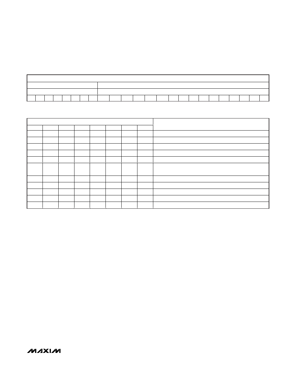
24-BIT SERIAL INPUT WORD
COMMAND BYTE
DATA BITS
MSB
LSB
C7 C6
C5 C4 C3
C2 C1 C0
D15
D14
D13
D12
D11
D10
D9
D8
D7
D6
D5
D4
D3
D2
D1
D0
Table 1. Input Command Bits
COMMAND BITS
C7
C6
C5
C4
C3
C2
C1
C0
OPERATION
X
X
X
X
0
0
0
0
No operation. Transfer shift register’s data to DOUT.
X
X
X
X
0
0
0
1
Write control register.
X
X
X
X
0
0
1
0
Read control register.
X
X
X
X
0
0
1
1
Load input register. DAC register unchanged.
X
X
X
X
0
1
0
0
Load DAC and input register.
X
X
X
X
0
1
0
1
Load DAC register. Transfer input register data to DAC
register. DAC outputs update on
CS’s rising edge.
X
X
X
X
0
1
1
0
Write clear register.
X
X
X
X
0
1
1
1
Read input register.
X
X
X
X
1
0
0
0
Read DAC register.
X
X
X
X
1
0
0
1
Read clear register.
X
X
X
X
1
1
1
1
No operation. Transfer shift register’s data to DOUT.
Table 2. Register Description
Register Descriptions
The MAX5661 communicates between its internal regis-
ters and the external bus lines through the 4-wire
SPI-/QSPI-/MICROWIRE-compatible serial interface.
Table 1 details the command bits (C7–C0) and the data
bits (D15–D0) of the serial input word. Tables 2 and 3
detail the command byte and the subsequent register
accessed. Tables 4–8 detail the various read/write
internal registers and their power-on reset states. When
updating the DAC register, allow 5µs before sending
the next command.
Control Register (Read/Write)
Write to the control register to enable the current or volt-
age output, set the voltage output for unipolar or bipolar
mode, and set the current-output range. The control
register also initializes the clear and fault modes. Set
the command byte to 0x01 to write to the control regis-
ter. Set the command byte to 0x02 to read from the
control register. Write or read data bits D15–D5. D4–D0
are don’t-care bits for a write operation. D4, D3, and D2
are read-only bits. D1 and D0 are don’t-care bits for a
read operation (see Table 4).
Set the OUTVON bit (D15) to 1 to enable the OUTV
DAC voltage output. Set the OUTION bit (D14) to 1 to
enable the OUTI DAC current output. Always set bit
D13 to 0. Set the B/U bit (D12) to determine whether the
OUTV output operates in bipolar mode (B/U = 0) or
unipolar mode (B/U = 1).
X = Don’t care. All other commands are reserved for factory use. Do not use.