Max5661, Pin description, Typical operating characteristics (continued) – Rainbow Electronics MAX5661 User Manual
Page 17
MAX5661
Pin Description
PIN
NAME
FUNCTION
1, 3, 5, 7, 8,
10, 15–20,
29–34, 36, 38,
42, 44, 46–52,
58, 61–64
N.C.
No Connection. Not internally connected.
2
OUTI
DAC Current-Source Output. OUTI sources either from 0 to 20mA or from 4–20mA.
4
V
DDI
DAC Current-Output Positive Supply. Connect V
DDI
to a power supply between +13.48V and
+40V to power the DAC current-output (OUTI) buffer. Bypass V
DDI
with a 0.1µF capacitor to
AGND, as close as possible to the device.
6
COMPI
OUTI Noise-Limiting Capacitor Connection. Connect a 22nF capacitor from COMPI to V
DDI
to
reduce transient noise at OUTI.
9
OUTI4/0
Current-Output Range Selection Input. Connect OUTI4/0 to AGND to select the 0 to 20mA OUTI
current-output range. Connect OUTI4/0 to VDDI to select the 4–20mA OUTI current-output range.
The OUTI current range can also be set by software. When using software to set the OUTI current
range, connect OUTI4/0 to AGND.
11
REF
Buffered Voltage Reference Input. Connect an external +4.096V voltage reference to REF. Bypass
REF with a 0.1µF capacitor to DACGND, as close as possible to the device. Use a 1k
Ω resistor in
series to the reference input for optimum performance.
12
DACGND
DAC Analog Ground. Connect DACGND, DACGNDS, DUTGND, and DUTGNDS together on a
low-noise ground plane with a star connection.
13
DACGNDS
DAC Analog Sense Ground. Connect DACGND, DACGNDS, DUTGND, and DUTGNDS together
on a low-noise ground plane with a star connection.
14
CNF1
Voltage/Current Configuration Input. CNF1 and CNF0 control the OUTV and OUTI outputs. See
Tables 13 and 14.
21
CNF0
Voltage/Current Configuration Input. CNF0 and CNF1 control the OUTV and OUTI outputs. See
Tables 13 and 14.
Single 16-Bit DAC with Current and Voltage
Outputs for Industrial Analog Output Modules
______________________________________________________________________________________
17
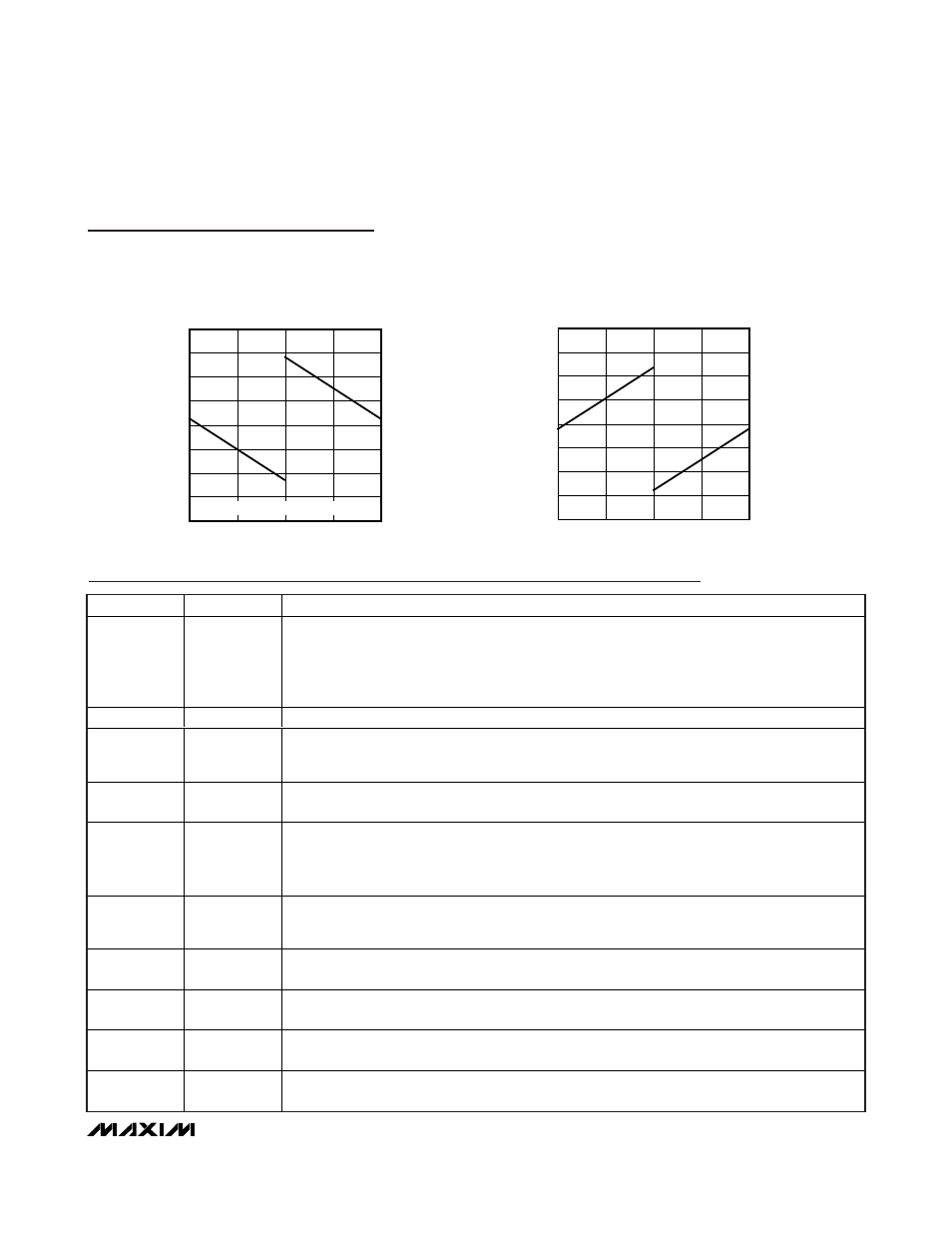
POSITIVE FULL-SCALE VOLTAGE
vs. FULL-SCALE OUTPUT TRIM CODE
MAX5661 toc65
CODE
FULL-SCALE VOLTAGE (V)
768
512
256
12
13
11
10
9
8
7
14
6
0
1024
UNIPOLAR OR BIPOLAR MODE
NEGATIVE FULL-SCALE VOLTAGE
vs. FULL-SCALE OUTPUT TRIM CODE
MAX5661 toc66
CODE
FULL-SCALE VOLTAGE (V)
768
512
256
-8
-7
-9
-10
-11
-12
-13
-6
-14
0
1024
Typical Operating Characteristics (continued)
(
Typical Operating Circuit, V
CC
= +5V, C
COMPI
= 22nF, V
DDV
= V
DDCORE
= +15V, V
SSV
= -15V, V
DDI
= +24V, V
REF
= +4.096V,
V
AGND
= V
DGND
= 0V, R
SERIES
= 47Ω, OUTV loaded with 2kΩ || 100pF to AGND, OUTI loaded with 500Ω to AGND, T
A
= +25°C.)