Acnodes FES 2213 User Manual
Page 49
Test Write Single Output Pi n
- Click the radio button-Single-P in.
- Key in the pin numbers you want to write. Pin numbers start from “0”.
- Key in the value either “0” or “1” in (R/W) Result fiel d to write the output pin you chose
above step.
- Click the WRITE GPIO DATA button to write the GP IO output pin.
Test Write Multiple Output Pi ns
- Click the radio button-M ultiple-Pins.
- Key in the pin number from “0x01” to “0x0F” to choose the multiple pin numbe rs to
write the value of the output pin. The pin numbers are ordered bitwise, i.e. bit 0
stands for GP IO 0, bit 1 stands for GPIO 1, etc. For exam ple, if you want to write pin 0,
1, and 3 , the pin numbe rs should be “0x0B”.
- Key in the value in (R/W) Result field from “ 0x01” to “0x0F” to write the value of the
output pin. The pin numbers are orde red bitwise, i.e . bit 0 stands for GPIO 0 , bit 1
stands for GP IO 1, etc. For example, if you want to set pin 0 and 1 high, 3 to low, the
pin numbe r should be “0x0B/, and then you should key in the value “0xxA” to write.
- Click the WRITE GPIO DATA button to write the GP IO output pins.
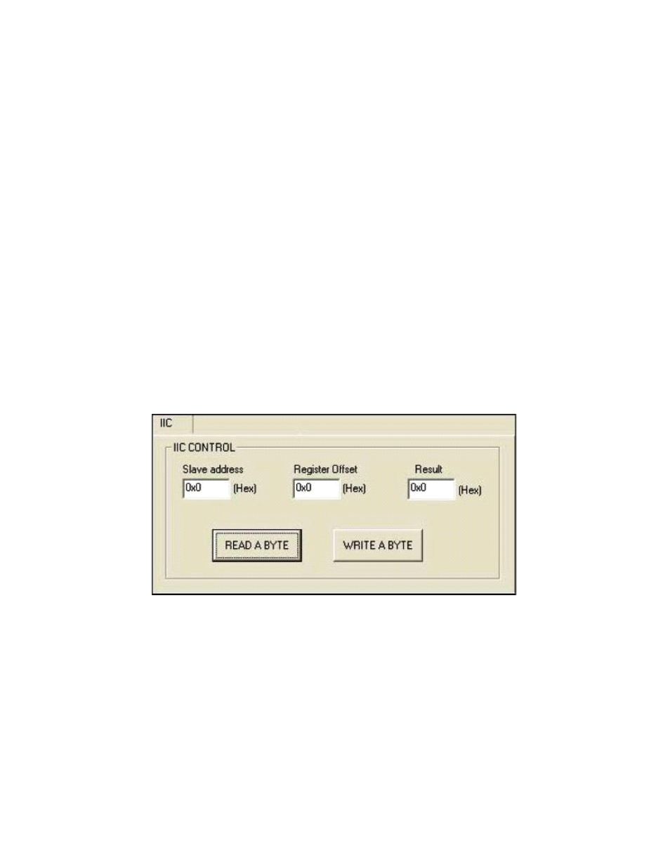
4-2.2 I²C
When the appl ication is executed, you can read or write a byte of data through I²C devices. All data must
be read or written in hexadecimal system.
Read a byte
- Key in the sl ave device address in Salve address fie ld.
- Key in the regi ster offset in Register Offset field.
- Click the READ A BYTE button and then a bute of data from the device wi ll be shown on
the Result field.