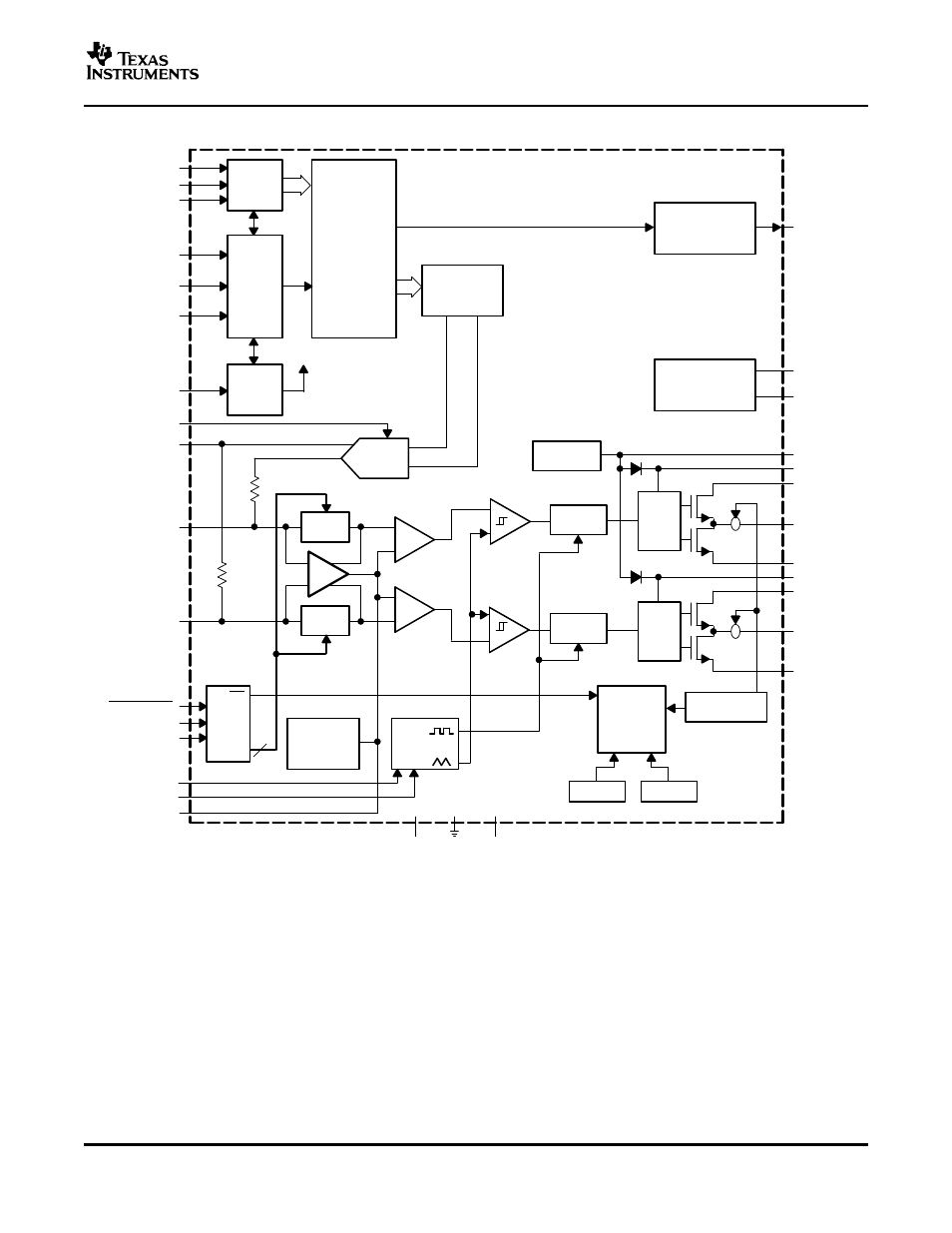
Functional block diagram – Texas Instruments TPA3200D1 User Manual
Page 5
www.ti.com
Audio
Serial
Port
Serial
Control
Port
4x/8x
Oversampling
Digital
Filter
and
Function
Control
Multi-Level
Delta-Sigma
Modulator
Audio
Serial
Port
System Clock
BCK
LRCK
DATA
FORMAT
MUTE
DEMP
SCLK
DAC and
2:1 Mux
LR_SEL
VCOM
Gain
Adjust
−
+
+
−
Gain
Adjust
FLT1
FLT2
_
+
_
+
_
+
_
+
Deglitch
Logic
Deglitch
Logic
Gate
Drive
Gate
Drive
Clamp
Reference
Short-Circuit
Detect
Start-Up
Protection
Logic
Thermal
V
CC
OK
SD
Gain
SHUTDOWN
GAIN0
GAIN1
2
Biases
and
References
Ramp
Generator
VREF AGND AVCC
VREF
AV
CC
Power Supply
Zero Detect
COSC
ROSC
BYPASS
ZERO
VDD
DGND
VCLAMP
BSN
PVCC
OUTN
PGND
BSP
OUTP
PGND
PVCC
TPA3200D1
SLOS442A – MAY 2005 – REVISED JULY 2005
Functional Block Diagram
5
See also other documents in the category Texas Instruments Receivers and Amplifiers:
- THS4151 (26 pages)
- TRF1500 (74 pages)
- SLOU082 (28 pages)
- TAS5508-5121K8EVM (24 pages)
- TPA6102A2 (16 pages)
- TPA3001D1EVM (22 pages)
- TPA6030A4 (25 pages)
- TPA701 (26 pages)
- TPA6110A2 MSOP (18 pages)
- TAS5727 (21 pages)
- THS4503EVM (28 pages)
- TPA005D02 (50 pages)
- SLOU121 (42 pages)
- TPA0243 (20 pages)
- TPA0253 (20 pages)
- TPA102 MSOP (26 pages)
- THS4131 (26 pages)
- SLOU020A (28 pages)
- TPA751 MSOP (20 pages)
- TPA005D12 (44 pages)
- TPA6139A2 EVM (8 pages)
- TPA0103 (32 pages)
- SLOU106 (26 pages)
- THS4141 (26 pages)
- THS3001 (20 pages)
- TPA0233 (20 pages)
- TPA2008D2 (26 pages)
- 2004 (20 pages)
- TPA3003D2 (36 pages)
- SLAU081 (44 pages)
- TPA301 (28 pages)
- TPA3100D2 (11 pages)
- SLOU023A (26 pages)
- TAS5110D6REF (45 pages)
- TA5704EVM (27 pages)
- TAS5518 (20 pages)
- APA100 (42 pages)
- TAS5066PAG (22 pages)
- TPA6204A1 (16 pages)
- THS4150 (26 pages)
- TPA311 (28 pages)
- TPA3008D2 (31 pages)
- TPA6101A2 (16 pages)