RAD Data comm ASMi-31 User Manual
Page 59
ASMi-31 Installation and Operation Manual
Appendix D. DTE Interface Connectors
General
D-3
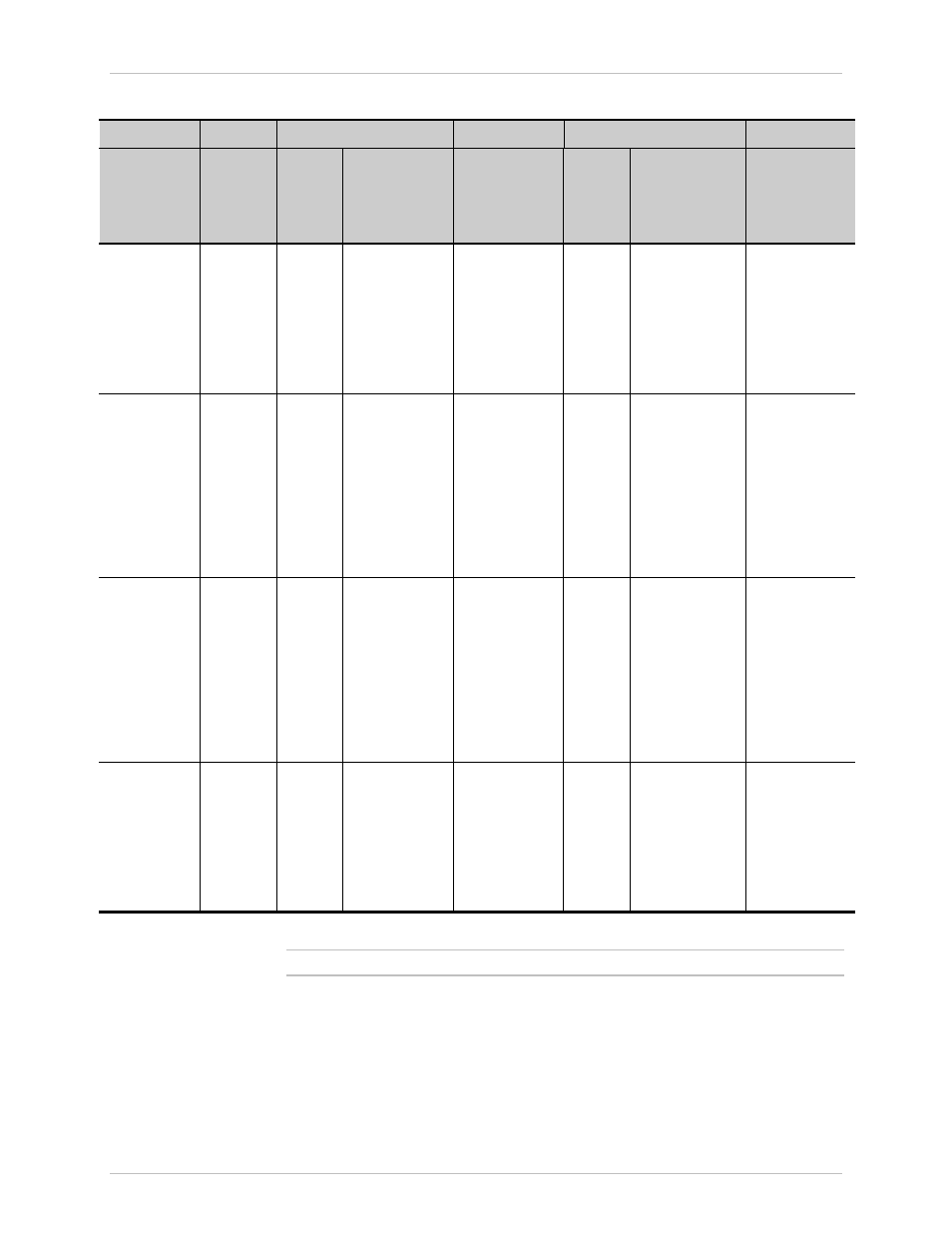
Table D-1 DTE Interface Signal Assignments (Cont.)
RS-232
V.35
EIA-530
X.21
Signal
Function
DB-25
Stand-
alone
and
Frame
DB-25
Frame
34-pin
Standalone
Pin Circuit
DB-25
Standalone
and Frame
Pin Circuit
DB-25
Frame
DB-15
Standalone
Pin Circuit/
(Function)
Description
External
Transmit
Clock
24
19
16
U SCTE(A) 113
W SCTE(B) 113
24
DA(A)
11
DA(B)
24
11
7
(A)*
14
(B)*
A serial data
rate clock input
from the data
source. Positive
clock
transitions must
correspond to
data transitions.
Transmit
Clock
15
14
10
Y SCT(A) 114
A SCT(B) 114
15
DB(A)
12
DB(B)
15
12
6
S(A)
13
S(B)
[SIGNAL
TIMING]
A transmit data
rate clock for
use by an
external data
source. Positive
clock
transitions
correspond to
data
transitions.
Receive Clock
17
22
23
X SCR(B) 115
V SCR(A) 115
17
DD(A)
9
DD(B)
A receive data
clock output
for use by
external data
sink. Positive
clock
transitions
correspond to
data
transitions.
Local Analog
Loop
18
18
L and j
141
18
LL
A control signal
input; when
on, commands
ASMi-31 into
Local Analog
Loopback
(V.54 Loop 3).
See Table 2-1.
Note
* Unassigned pins according to X.21 standard.
Order from: Cutter Networks
Ph:727-398-5252/Fax:727-397-9610
www.bestdatasource.com