6 extension connector (j7), Operational specifications – Renesas M3A-HS25 User Manual
Page 34
Operational Specifications
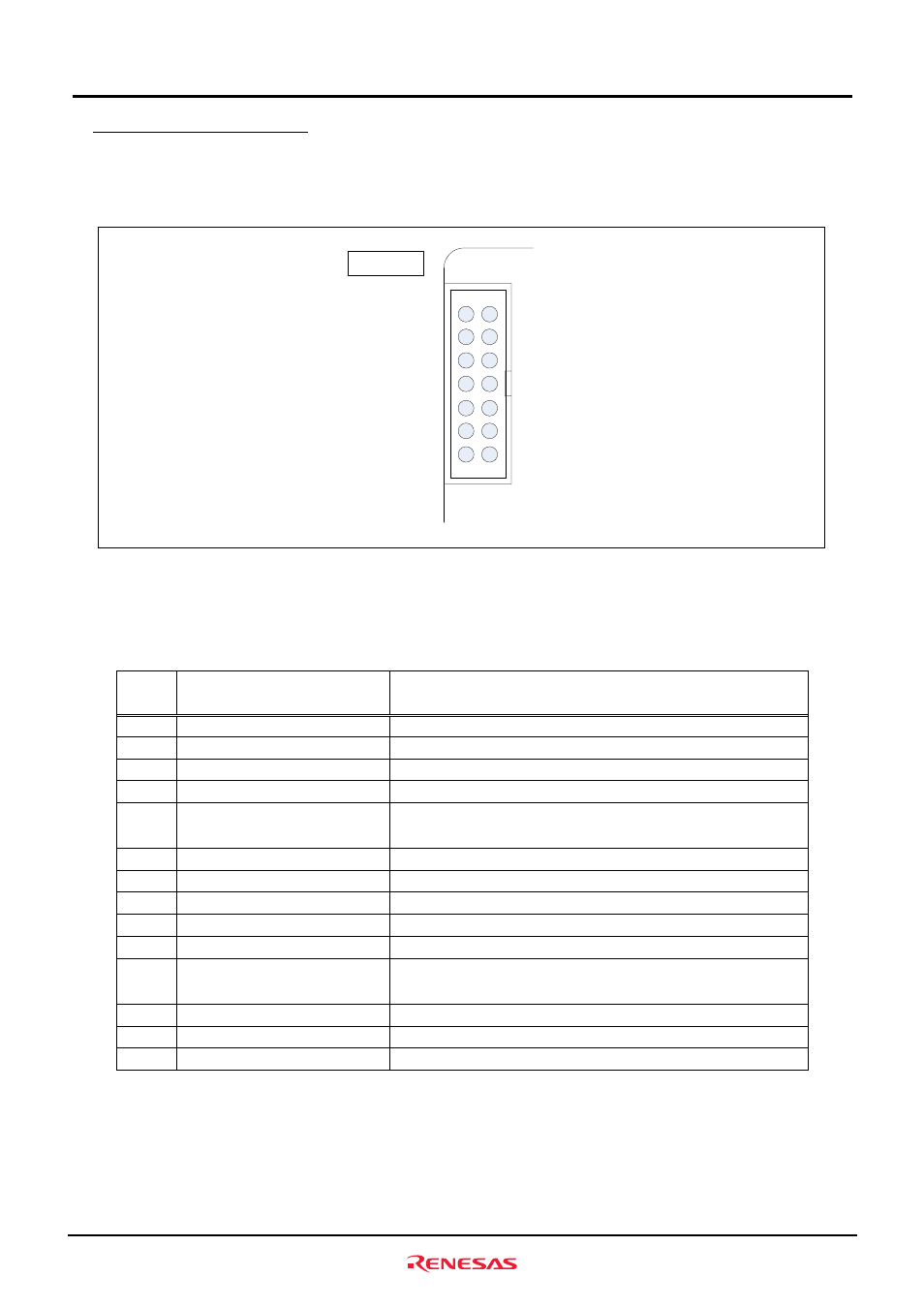
3.1.6 Extension Connector (J7)
3
3.1.6 Extension Connector (J7)
Extension connector(J7) connects the pins necessary for writing a on-chip flash memory of SH7125.
Figure 3.1.7 shows pin assignments of the extension connectors.
13
14
11
12
9
10
7
8
5
6
3
4
1
2
Board
edge
Top view of the
component side
J7
Board
edge
Figure 3.1.7 Pin assignments of the Extension Connector (J7)
Table 3.1.7 lists pin assignments of the extension connector(J7).
Table 3.1.7 Pin assignments of the extension connector (J7)
Pin
J7
Signal name
Other connection
1
PA5/IRQ3/SCK1
Extension connector (J6)
2
GND -
3
NC
-
4
MD1
DIP switch for system setting (SW4-2)
5
PA4/IRQ2/TXD1/TMS
H-UDI connector (J1), Serial Port Select Jumper (JP3), Extension
connector (J5)
6
NC -
7
FWE/ASEBRK
______________
/ASEBRKAK
___________________
*
DIP switch for system setting (SW4-1)
8
VCC -
9
PA6/TCLKA
Extension connector (J5)
10
NC -
11
PA3/IRQ1/RXD1/TRST
_________
H-UDI connector (J1), Serial Port Select Jumper (JP4), Extension
connector (J5)
12
NC -
13
RESET
____________
Reset module
14
GND -
Note *
:
When FWE pin select jumper (JP2) is set to “2-3”, it is activated.
Rev.1.0 July 21, 2006
3-10
REJ10J0952-0100