7 m3a-hs25 memory mapping – Renesas M3A-HS25 User Manual
Page 12
Overview
1.7 M3A-HS25 Memory Mapping
Rev.1.0 July 21, 2006
1-8
REJ10J0952-0100
1
1.7 M3A-HS25 Memory Mapping
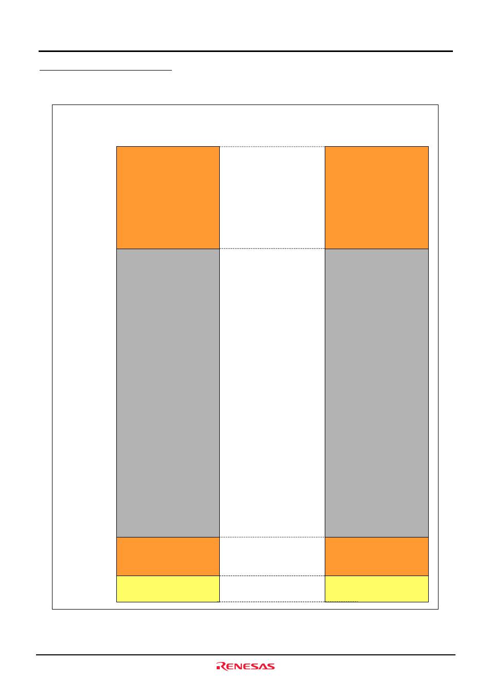
Figure1.7.1 show a memory mapping example of SH7125 in the M3A-HS25.
Reserved
Logical space of the SH7125
MCU mode 3
(Single Chip mode)
On-chip RAM
(8KB)
On-chip Peripheral Module
H’0000 0000
H’0001 FFFF
H’0002 0000
H’FFFF 9FFF
H’FFFF A000
H’FFFF BFFF
H’FFFF C000
H’FFFF FFFF
Memory Mapping
of the M3A-HS25
On-chip Peripheral Module
H’0000 0000
Reserved
H’FFFF FFFF
On-chip ROM
(128KB)
On-chip ROM
(128KB)
H’0001 FFFF
H’0002 0000
On-chip RAM
(8KB)
H’FFFF 9FFF
H’FFFF A000
H’FFFF BFFF
H’FFFF C000
Figure1.7.1 Memory Mapping Example of SH7125 (MCU mode 3)
See also other documents in the category Renesas Hardware:
- Single-Chip Microcomputer M34551T2-MCU (42 pages)
- M3T-FLX-80NRA (6 pages)
- 70 (162 pages)
- M16C/30P (102 pages)
- PROM Programming Adapter PCA7427G02 (20 pages)
- R0E572110CFK00 (40 pages)
- H8/325 Series (20 pages)
- Single-Chip Microcomputer H8/36079 (27 pages)
- Direct Dummy IC M3T-DIRECT100S (4 pages)
- M3A-2152 (95 pages)
- PCA7755D (6 pages)
- M16C/6N5 (106 pages)
- SH7085 (50 pages)
- QFP-144 (23 pages)
- H8/3834 Series (22 pages)
- RSKM16C62P (3 pages)
- H8/33937 (22 pages)
- Single-Chip Microcomputer H8SX/1622 (5 pages)
- E6000 (29 pages)
- PCA7400 (18 pages)
- PCA4738FF-64 (20 pages)
- SuperH HS7339KCU01HE (43 pages)
- M16C FAMILY (103 pages)
- PCA7412F-100 (20 pages)
- 4513 (210 pages)
- M34551E8FP (16 pages)
- Dummy IC M3T-SSOP36B-450 (4 pages)
- Emulation Pod M30100T3-RPD-E (52 pages)
- Converter Board for M30102 M30102T-PTC (4 pages)
- SH7145 (31 pages)
- HS1653ECN61H (36 pages)
- Converter Board R0E521276CFG00 (4 pages)
- PCA7302E1F-80 (18 pages)
- H8/3814 Series (21 pages)
- H8S/2646 Series (20 pages)
- SuperHTM Family SH7125 Series (40 pages)
- M30262T-PTC (4 pages)
- SH7670 (82 pages)
- H8/3864 Series (20 pages)
- Emulator System M3T-MR100 (306 pages)
- 38K0 (6 pages)
- PLQP0176KB-A (40 pages)
- Direct Dummy IC M3T-DIRECT80S (6 pages)
- PCA4738L-80A (26 pages)
- Converter Board R0E5212BACFG00 (6 pages)