7 serial rom interface signals – Ricoh R5C841 User Manual
Page 70
R5C841 PCI-CardBus/IEEE 1394/SD Card/Memory Stick/xD/ExpressCard Data Sheet
12345
2004
R
EV
. 1.10
5-17
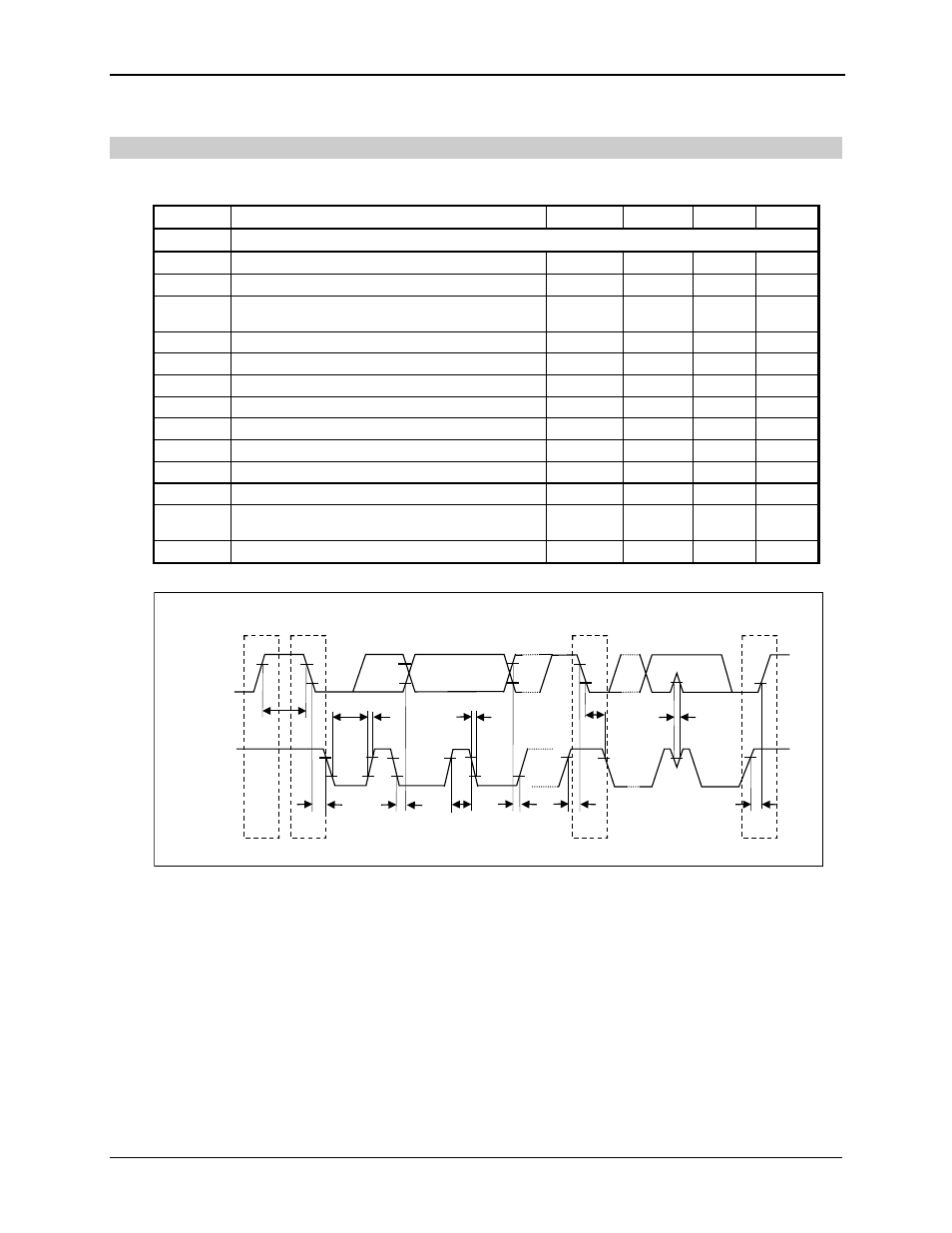
5.3.7 Serial ROM Interface signals
SDA (UDIO4), SCL(UDIO3)
(VCC_ROUT= 1.65~1.95V, VCC_3V=3.0~3.6V, Ta=0~70ºC)
Symbol Parameter Min
Max
Unit
Note
SDA (UDIO4), SCL (UDIO3)
f
SCL
SCL clock frequency
0
100
kHz
t
BUF
Bus free time between a STOP and START condition
4.7
-
us
t
HD;STA
Hold time (repeated) START condition. After this
period, the first clock pulse is generated
4.0 - us
t
LOW
LOW period of the SCL clock
4.7
-
us
t
HIGH
HIGH period of the SCL clock
4.0
-
us
t
SU;STA
Set–up time for a repeated START condition
4.7
-
us
t
HD;DAT
Data hold time for I
2
C–bus devices
0
us
t
SU;DAT
Data set–up time
250
-
ns
t
R
Rise time of both SDA and SCL signals
-
1000
ns
t
F
Fall time of both SDA and SCL signals
-
300
ns
t
SU;STO
Set–up time for STOP condition
4.0
-
us
t sp
Pulse width of spikes which must be suppressed by
the input filter
n/a n/a ns
C
b
Capacitive load for each bus line
-
400
pF
All values referred to V IHmin and V ILmax levels (see 5.2.11).
Serial ROM if SDA,SCL timing
SDA(UDIO4)
S
P
t
HD;STA
t
HD;DAT
t
SP
t
R
t
LOW
t
BUF
SCL(UDIO3)
t
SU;DAT
t
HIGH
t
SU;STA
t
HD;STA
t
F
t
SU;STO
Sr
P