NEC PD75P308 User Manual
Page 26
µ
PD75P308
26
*1: These symbols are the corresponding
µ
PD27C256 symbols.
2: The internal address signal is incremented by 1 at the fourth rising edge of X1 input. The internal
address is not connected to any pin.
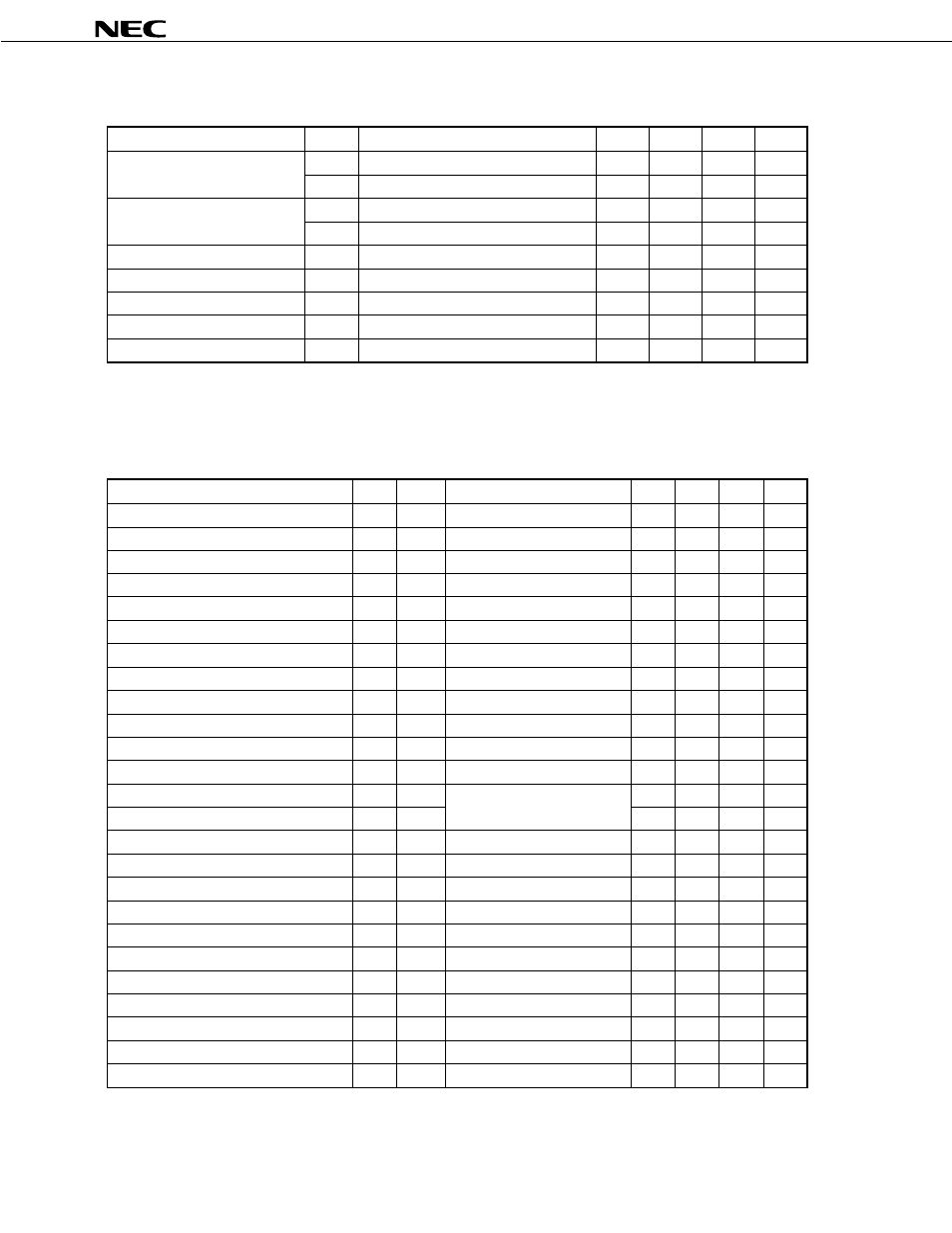
Parameter
Symbol
*
1
Conditions
MIN.
TYP.
MAX.
Unit
t
AS
t
AS
t
M1S
t
OES
t
DS
t
DS
t
AH
t
AH
t
DH
t
DH
t
DF
t
DF
t
VPS
t
VPS
t
VDS
t
VCS
t
PW
t
PW
t
OPW
t
OPW
t
MOS
t
CES
t
DV
t
DV
t
M1H
t
OEH
t
M1R
t
OR
t
PCR
–
t
XH
,t
XL
–
f
X
–
t
I
–
t
M3S
–
t
M3H
–
t
M3SR
–
t
DAD
t
ACC
t
HAD
t
OH
t
M3HR
–
t
DFR
–
MD0 = MD1 = V
IL
t
M1H
+ t
M1R
≥
50
µ
s
When data is read from program memory
When data is read from program memory
When data is read from program memory
When data is read from program memory
When data is read from program memory
2
µ
s
2
µ
s
2
µ
s
2
µ
s
2
µ
s
0
130
ns
2
µ
s
2
µ
s
0.95
1.0
1.05
ms
0.95
21.0
ms
2
µ
s
1
µ
s
2
µ
s
2
µ
s
10
µ
s
0.125
µ
s
4.19
MHz
2
µ
s
2
µ
s
2
µ
s
2
µ
s
2
µ
s
0
130
ns
2
µ
s
2
µ
s
Address Set-Up Time
*2
(vs.MD0
↓
)
MD1 Set-Up Time (vs. MD0
↓
)
Data Set-Up Time (vs. MD0
↓
)
Address Hold Time
*2
(vs.MD0
↑
)
Data Hold Time (vs. MD0
↑
)
MD0
↑→
Data Output Float Delay Time
V
PP
Set-Up Time (vs. MD3
↑
)
V
DD
Set-Up Time (vs. MD3
↑
)
Initial Program Pulse Width
Additional Program Pulse Width
MD0 Set-Up Time (vs. MD1
↑
)
MD0
↓→
Data Output Delay Time
MD1 Hold Time (vs. MD0
↑
)
MD1 Recovery Time (vs. MD0
↓
)
Program Counter Reset Time
X1 Input High-/Low- Level Width
X1 Input Frequency
Initial Mode Set Time
MD3 Set-Up Time (vs. MD1
↑
)
MD3 Hold Time (vs. MD1
↓
)
MD3 Set-Up Time (vs. MD0
↓
)
Address
*2
→
Data Output Delay Time
Address
*2
→
Data Output Hold Time
MD3 Hold Time (vs. MD0
↑
)
MD3
↓→
Data Output Float Delay Time
Notes 1: V
PP
must not exceed +13.5 V, including the overshoot.
2: Apply V
DD
before V
PP
and disconnect it after V
PP
.
Parameter
Symbol
Conditions
MIN.
TYP.
MAX.
Unit
0.7 V
DD
V
DD
V
V
DD
–0.5
V
DD
V
0
0.3 V
DD
V
0
0.4
V
10
µ
A
V
DD
–1.0
V
0.4
V
30
mA
30
mA
Other than X1 or X2
X1 and X2
Other than X1 or X2
X1 and X2
V
IN
= V
IL
or V
IH
I
OH
= –1 mA
I
OL
= 1.6 mA
MD0 = V
IL
, MD1 = V
IH
V
IH1
V
IH2
V
IL1
V
IL2
I
LI
V
OH
V
OL
I
DD
I
PP
High-Level Input Voltage
Low-Level Input Voltage
Input Leakage Current
High-Level Output Voltage
Low-Level Output Voltage
V
DD
Supply Current
V
PP
Supply Current
AC PROGRAMMING CHARACTERISTICS (T
a
= 25
±
5
°
C, V
DD
= 6.0
±
0.25V, V
PP
= 12.5
±
0.3V, V
SS
= 0V)
DC PROGRAMMING CHARACTERISTICS (T
a
= 25
±
5
°
C, V
DD
= 6.0
±
0.25V, V
PP
= 12.5
±
0.3V, V
SS
= 0V)
★
★