Program memory read procedure – NEC PD75P308 User Manual
Page 13
µ
PD75P308
13
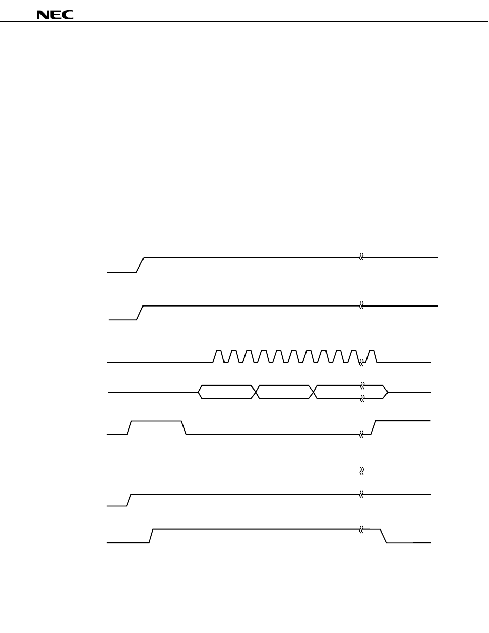
3.3 PROGRAM MEMORY READ PROCEDURE
The contents of the program memory can be read in the following procedure.
(1) Ground the unused pins through pull-down resistors. The X1 pin must be low.
(2) Supply 5 V to the V
DD
and V
PP
pins.
(3) Wait for 10 microseconds.
(4) Set program memory address 0 clear mode.
(5) Supply 6 V to the V
DD
pin and 12.5 V to the V
PP
pin.
(6) Set program inhibit mode.
(7) Set verify mode. Data of each address is sequentially output each time a clock pulse is input to the
X1 pin four times.
(8) Set program inhibit mode.
(9) Set program memory address 0 clear mode.
(10) Change the voltages of V
DD
and V
PP
pins to 5 V.
(11) Turn off the power supply.
Steps (2) to (9) are illustrated below.
V
PP
V
DD
V
DD
+1
V
DD
V
PP
V
DD
Data output
Data output
P40-P43
P50-P53
MD0
(P30)
MD1
(P31)
MD2
(P32)
MD3
(P33)
X1
- Express 320Lc (4 pages)
- Express5800/120Rh-2 N8100-1125F (406 pages)
- Express NR579-02 (10 pages)
- 140He (360 pages)
- Esmpro EXP350E (2 pages)
- MATWORX NWA-008862-001 (66 pages)
- 1320Xd (20 pages)
- 5020M-16 (149 pages)
- NECCare Standard/300 (11 pages)
- Express 5800/320Lb-R (302 pages)
- Express 5800/320Lc-R (357 pages)
- EXPRESS5800/100 SERIES N8100-1635F (152 pages)
- ExpressA1160 (252 pages)
- EXPRESS 320Lb (39 pages)
- NEAX2000 ND-91649 (58 pages)
- Server Express5800 (400 pages)
- NX7700i/5080H-32 (170 pages)
- EXP351E (2 pages)
- 5800 Series (12 pages)
- Express320F (2 pages)
- 320Fc (120 pages)
- set810 (2 pages)
- NEAX NDA-24349 (421 pages)
- Express5800 Series N8800-090F (358 pages)
- L320 (198 pages)
- Express 456-01721-000 (26 pages)
- INTEL 5800/1000 (12 pages)
- Care Express5800/FT (14 pages)
- Express5800/340Hb-R (4 pages)
- R320A-E4 (23 pages)
- Express 320Fc Systems (10 pages)
- Express 5800/230Eh (342 pages)
- Express N8800-063E/064E (145 pages)
- EXPRESS800 (78 pages)
- MH4500 (186 pages)
- NEAX 2000 IPS (96 pages)
- 2000 (137 pages)
- MC2400 (204 pages)
- Express120Bb-6 (2 pages)
- EXPRESS 320Lb-R (296 pages)
- 120Rf-2 (20 pages)
- A1160 (62 pages)
- 1080Xd (216 pages)