NEC PD75P308 User Manual
Page 18
µ
PD75P308
18
Ports 2, 3
Ports 0, 1, 6, 7, RESET
Ports 4, 5
Open-drain
X1, X2, XT1
Ports 2, 3, 4, 5
Ports 0, 1, 6, 7, RESET
X1, X2, XT1
Ports 0, 2, 3,
I
OH
= -1mA
6, 7
BIAS
BP0-7
I
OH
= -100
µ
A*
1
Ports 0, 2, 3,
Ports 3, 4, 5
6, 7
I
OL
= 15mA
I
OL
= 1.6mA
SB0, 1
Open-drain
BP0-7
I
OL
= 100
µ
A*
1
Other than below
X1, X2, XT1
V
IN
= 10V
Ports 4, 5
Other than below
X1, X2, XT1
V
OUT
= V
DD
Other than below
V
OUT
= 10V
Ports 4.5
V
OUT
= 0V
Ports 0, 1, 2, 3, 6, 7
(except P00) V
IN
= 0V
V
LCD0
= V
LCD
V
LCD1
= V
LCD
x —
V
LCD2
= V
LCD
x —
2.7 V
≤
V
LCD
≤
V
DD
*
6
HALT mode
HALT mode
V
IH1
V
IH2
V
IH3
V
IH4
V
IL1
V
IL2
V
IL3
V
OH2
V
OL1
V
OL3
I
LIH1
I
LIH2
I
LIH3
I
LIL1
I
LIL2
I
LOH1
I
LOH2
I
LOL
V
LCD
I
DD1
I
DD2
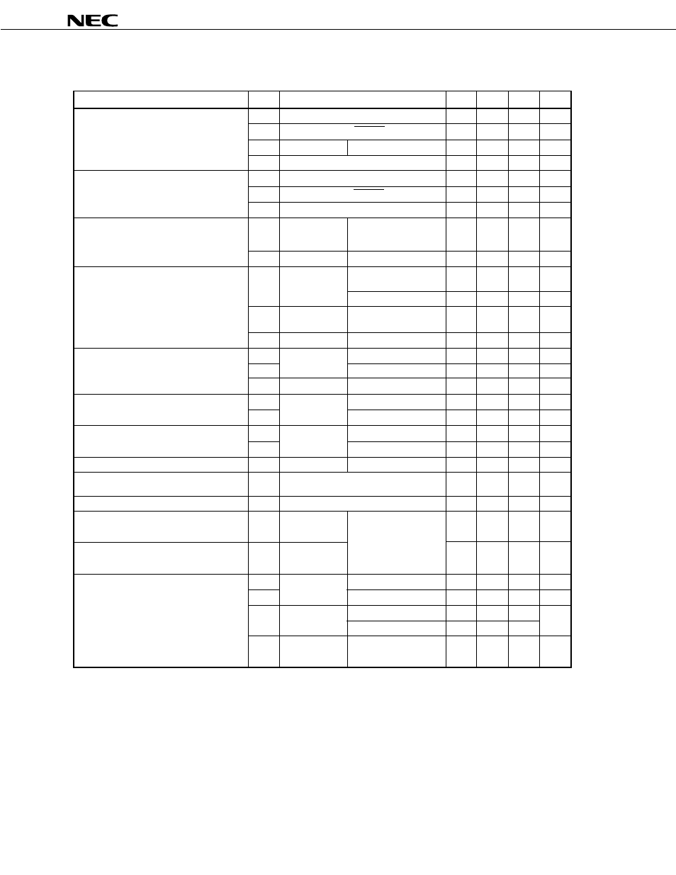
High-Level Input Voltage
Low-Level Input Voltage
High-Level Output Voltage
Low-Level Output Voltage
High-Level Input Leakage Current
Low-Level Input Leakage Current
High-Level Output Leakage Current
Low-Level Output Leakage Current
Internal Pull-Up Resistor
LCD Drive Voltage
LCD Output Voltage Deviation
(Common)
LCD Output Voltage Deviation
(Segment)
Supply Current
0.7 V
DD
V
DD
V
0.8 V
DD
V
DD
V
0.7 V
DD
10
V
V
DD-
0.5
V
DD
V
0
0.3 V
DD
V
0
0.2 V
DD
V
0
0.4
V
V
DD-
1.0
V
DD-
2.0
V
0.4
V
1.0
V
3
µ
A
20
µ
A
20
µ
A
-3
µ
A
-20
µ
A
3
µ
A
20
µ
A
-3
µ
A
2.5
V
DD
V
5
15
mA
500
1500
µ
A
350
1000
35
100
DC CHARACTERISTICS (T
a
= -10 to +70
°
C, V
DD
= 5V
±
5%)
Parameter
Symbol
Conditions
MIN.
TYP.
MAX.
Unit
0.4
2.0
V
0.2V
DD
V
Pull-up R
≥
1k
Ω
V
IN
= V
DD
V
IN
= 0V
V
ODC
V
ODS
I
0
=
±
5
µ
A
0
±
0.2V
V
I
0
=
±
1
µ
A
0
±
0.2V
V
2
3
1
3
µ
A
15
40
80
K
Ω
0.5
20
µ
A
XT1 = 0V
STOP mode
4.19MHz crystal
*
4
oscillator
C1 = C2 = 22pF
32 kHz
*
5
crystal oscillator
*
3
*
2
*
2
* 1: When using two of BP0-BP3 and two of BP4-BP7 for output at the same time.
2: "Voltage deviation" means the difference between the ideal segment or common output value
(V
LCD
n: = 0, 1, 2) and output voltage.
3: Currents for the built-in pull-up resistor are not included.
4: Including when the subsystem clock is operated.
5: When operated with the subsystem clock by setting the system clock control register (SCC) to
1001 to stop the main system clock operation.
6: When operand in the high-speed mode with the processor clock control register (PCC) set to 0011.
V
OH1
V
V
OL2
R
LI
I
DD3
I
DD4