Chapter 2 hardware overview of the ni 781xr, Figure 2-1. ni 781xr block diagram, Chapter 2 hardware overview of the ni 781 x r – National Instruments NI 781xR User Manual
Page 19: Hardware overview of the ni 781 x r
© National Instruments Corporation
2-1
2
Hardware Overview
of the NI 781xR
This chapter presents an overview of the hardware functions and
I/O connectors on the NI 781xR.
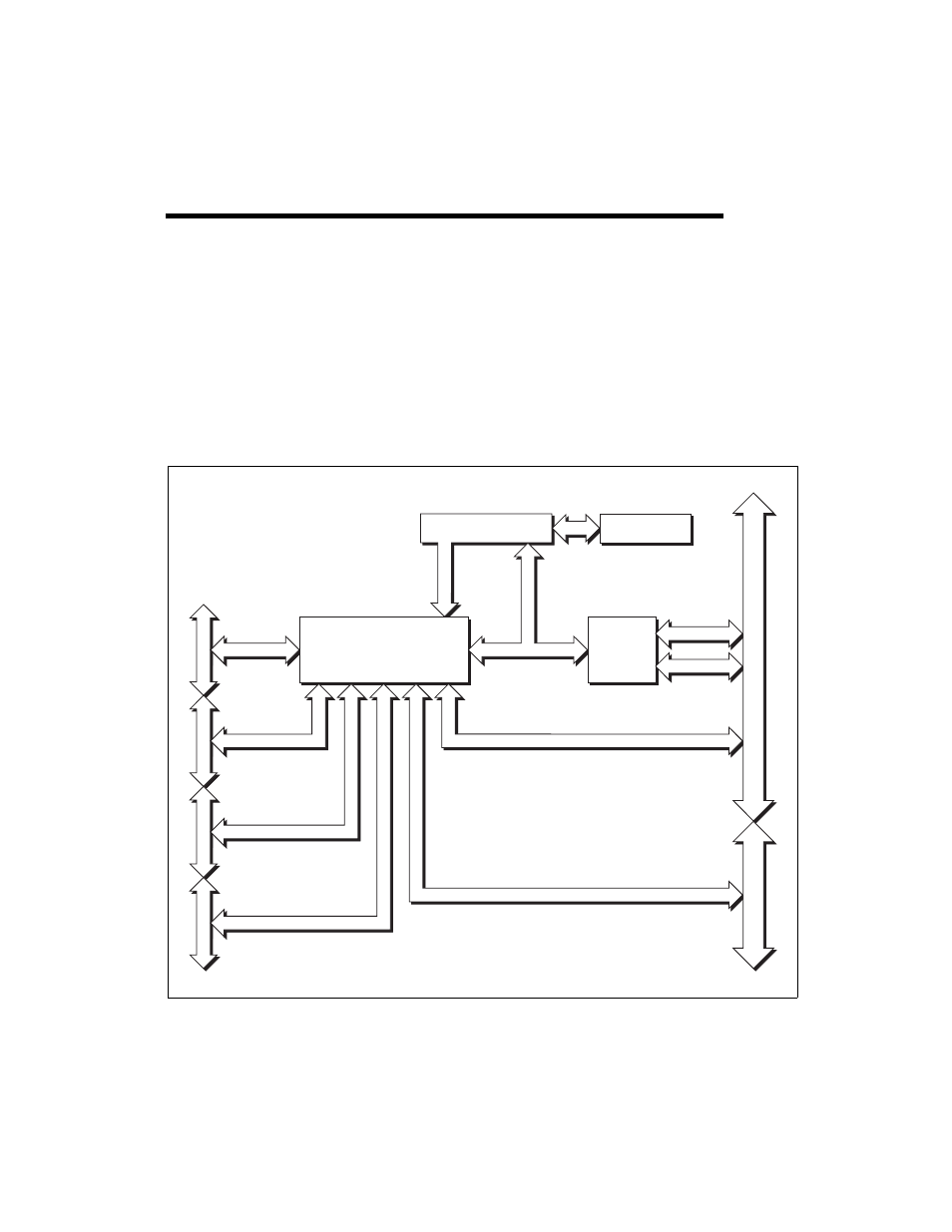
Figure 2-1 shows a block diagram for the NI 781xR.
Figure 2-1. NI 781xR Block Diagram
Configur
ation
Configuration Control
Connector 0 (DIO)
Connector 1 (DIO)
Connector 2 (DIO)
Connector 3 (DIO)
Digital I/O (40)
User-Configurable
FPGA on
RIO Devices
Digital I/O (40)
Digital I/O (40)
Digital I/O (40)
Data/Address/Control
Bus
Interface
Address/Data
Control
Flash Memory
PCI/PXI/CompactPCI Bus
R
TSI/PXI T
riggers
PXI Local Bus (NI PXI-781x R Only)
RTSI Bus
See also other documents in the category National Instruments Hardware:
- Instrument Driver NI-DMM (12 pages)
- 24-Bit Half/Full-Bridge Analog Input Module NI 9237 (36 pages)
- NI PXIe-8105 (76 pages)
- PXI NI 5401 (60 pages)
- Fieldpoint CFP-2210 (38 pages)
- NI 6233 (180 pages)
- 6508 PCI-DIO-96 (93 pages)
- PXI/CompactPCI Embedded Computer NI PXI-8108 (83 pages)
- NI 9233 (34 pages)
- NI USB-9219 (25 pages)
- GPIB-PC (262 pages)
- cFP-RTD-122 (15 pages)
- USB device 625x (23 pages)
- Isolated Analog Input Modules SCC-AI01 (18 pages)
- NI PCI-6111 (118 pages)
- NI USB-6008 (32 pages)
- PC-DIO-24 (75 pages)
- NI 9474 (31 pages)
- NI 6013 (109 pages)
- PXI-1428 (46 pages)
- NI PCI-5911 (51 pages)
- 2 SD Card Memory Module NI 9802 (16 pages)
- cFP-20xx (24 pages)
- NI USB-9234 (23 pages)
- NI 9871 (24 pages)
- Interface Device NI PCI-1426 (35 pages)
- AT E Series (184 pages)
- 9211A (19 pages)
- Module NI PXI-8250 (39 pages)
- 8330 Series (30 pages)
- NI PXIe-8360 (40 pages)
- Deterministic Ethernet Expansion Chassis NI 9144 (65 pages)
- NI 6509 (23 pages)
- NI MATRIXx Xmath (127 pages)
- NI 9481 (23 pages)
- Monochrome Image Acquisition Device NI 1410 (34 pages)
- VXI-1394 (74 pages)
- NI PXI-8104 (69 pages)
- NI 9235 (38 pages)
- 370620B-01 (17 pages)
- FP-RTD-124 (15 pages)
- VXI-USB (61 pages)
- NI PCI-8254R (45 pages)
- Interface Device NI PCI-8254R (16 pages)