SMC Networks SMC91C95 User Manual
Page 108

108
TIMING DIAGRAMS
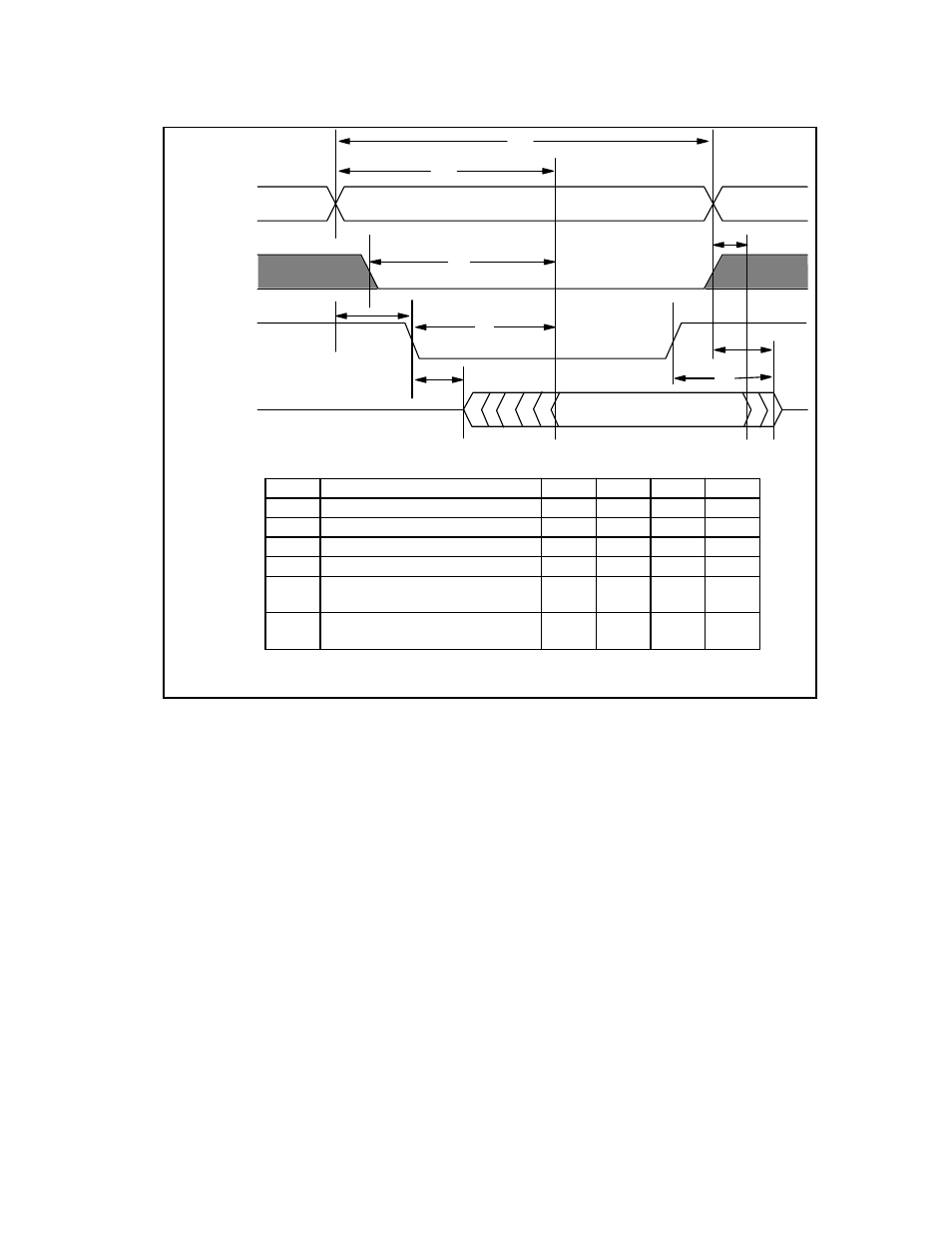
FIGURE 18 - PCMCIA MEMORY READ TIMING
A[5:0], nREG
nCE1
nOE
D[15:0]
DATA VALID
t1
t2
t3
t4
t5
t6
0 min
30 max
5 max
Parameter
Min
Typ
Max
Units
t1
Address Access Time
300
ns
t2
nREG Access Time
300
ns
t3
nCE1 Access Time
300
ns
t4
nOE Access Time
150
ns
t5
Output Disable Time from
nCE1 high
100
ns
t6
Output disable Time from nOE
high
100
ns
NOTE: Applies only when nWAIT is asserted by the SMC91C95.
See also other documents in the category SMC Networks Hardware:
- EZ Connect SMC8414-2P-SIP (2 pages)
- SMCWPCI-G (2 pages)
- SMC EZ Connect 2.4GHz 11 Mbps Wireless USB Flash Drive SMCWUSB32 (45 pages)
- TIGERCARD SMC10GPCIE-XFP (35 pages)
- SMC EZ Connect g SMCWCBT-G (32 pages)
- SMC EZ Connect Wireless Print Server with USB Port SMCWPS-G (2 pages)
- Barricade SMCBR 18VPN (73 pages)
- SMCHP1D-ETH (26 pages)
- Barricade SMC7404BRA EU (130 pages)
- SMC8002CM-U (2 pages)
- SMC9432TX/MP (76 pages)
- SMC2635W (42 pages)
- SMC10GPCIe-10BT (2 pages)
- SMCBGSSCX1 (1 page)
- EZ Connect SMC8014-TES (2 pages)
- SMC1211TX (15 pages)
- EZ Card 10/100 10/100 Mbps Fast Ethernet PCI Card with Wake-On-LAN SMC1255TX-1 (2 pages)
- SMCWBR 14-GM (69 pages)
- BARRICADE SMCWBR14-N2 (103 pages)
- Barricade SMC7004AWBR (94 pages)
- EZCONNECT SMCWUSB-N2 (2 pages)
- EtherNet/IP EX500-GEN1 (23 pages)
- SMCWEBT-G (66 pages)
- Barricade SMC2404WBR (134 pages)
- SMC EliteConnect SMC2586W-G (96 pages)
- SMC EZ Connect SMC2821USB (2 pages)
- 486DX (81 pages)
- SMC7908VoWBRA (137 pages)
- SMCWAA-B (51 pages)
- SMCWUSBS-N (64 pages)
- EZ Networking SMC2209USB/ETH (17 pages)
- 5MC2671W (76 pages)
- SMC Barricade SMCBR24Q (94 pages)
- Tiger Access Extended Ethernet Splitter SMC7048/VSP (2 pages)
- Wireless Broadband Router (50 pages)
- SMC7003-USB (2 pages)
- SMC Barricade SMCBR14UP (2 pages)
- SMC Barricade g SMC2804WBR (114 pages)
- ARM AHB SRAM/NOR (110 pages)
- SMC7004VBR V.2 (61 pages)
- SMC EliteConnect SMC2512W-B (2 pages)
- Barricade SMCWBR14-G (105 pages)
- SMC3056IM V5 (12 pages)
- THE BARRICADE SMCWBR14S-N4 (2 pages)
- Barricade Cable/DSL Router (40 pages)
