Power supply circuits, 4 power supply circuits (main unit) – Icom IC-F5061 User Manual
Page 12
5 - 4
PLL IC
The PLL circuit provides stable oscillation of the transmit
frequency and receive 1st LO frequency. The PLL output
frequency is controlled by the divided ratio (N-data) from the
CPU.
The applied signals are divided at the prescaler and
programmable counter according to the control signals
(“SSO,” “PLST” and "SCK”) from the CPU. The divided signal
is phase-compared with the reference frequency signal from
the reference frequency oscillator (X1, pin 3), at the phase
detector.
The phase difference is output from pin 4 as a pulse type
signal after being passed through the internal charge pump.
The output signal is converted into the DC voltage (lock
voltage) by passing through the loop filter (Q8, Q9). The lock
voltage is applied to the variable capacitors (D10 and D13
of RX VCO1, D8 and D9 of RX VCO2, D14 and D17 of TX
VCO), and locked to keep the VCO frequency constant.
If the oscillated signal drifts, its phase changes from that of
the reference frequency, causing a lock voltage change to
compensate for the drift in the VCO oscillating frequency.
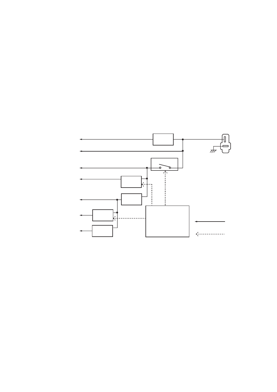
CPU5
regurator
+8V
regurator
R8V
regurator
Power switch
Q47, Q48
IC18
IC20
Q38, Q39
HV
HV
VCC
“PW
ON”
CPU5
CPU
+8V
+5V
regurator
Q35, Q36
+5V
Voltage line
Control signal
41
46
47
“RXC”
“TXC”
R8V
Receiver circuits
Common circuits
CPU (IC14),
EEPROM (IC16),
etc.
RF power amplifier (IC15)
etc.
AF power amplifier (IC21)
etc.
PLL IC (IC4)
Transmitter circuits
(IC14)
Attached optional units,
D/A converters,
etc.
Power Supply
• POWER SUPPLY CIRCUITS
T8V
regurator
Q34, Q37, D37
T8V
5-4 POWER SUPPLY CIRCUITS (MAIN UNIT)
Voltage from the attached battery pack is routed to whole of the circuit in the transceiver via switches and regulators.