Circuit description, Receiver circuits, 1 receiver circuits – Icom IC-F5061 User Manual
Page 9

5 - 1
SECTION 5
CIRCUIT DESCRIPTION
5-1 RECEIVER CIRCUITS
RF CIRCUITS
The antenna switching circuit toggles between the receive
(RX) line and transmit (TX) line. RF amplifi er amplifi es the
received signals within the frequency coverage.
Received signals from the antenna are passed through Low
Pass filter (LPF; L40, C369, C370), TX power detector (D47,
D49, D51) and another LPF (L38, L39, C343, C345, C356,
C357), then applied to the antenna switching circuit (D38/
D39, L37, C337, C346).
The received signals are passed through the antenna
switching circuit as an LPF (L37, C337, C346), LPF (L35,
C322, C322, C323, C336) and two-staged tuned Bandpass
Filter (BPF; D34, L32, C299, C300 and D31, L31, C278,
C279), then applied to the RF amplifier (Q31).
The amplified signals are passed through another two-
staged tuned BPF (D27, L28, C260−C263, C242 and D26,
L26, C219, C220, C240) and applied to the 1st mixer (IC10;
pins 4, 5, L18, L19, L24).
1ST IF CIRCUITS
The amplified received signals from the RF circuit are
converted into the 1st IF signal, fi ltered and amplifi ed at the
1st IF circuits.
The received signals from the RF circuits are mixed with
1st Local Oscillator (LO) signal from the RX VCOs, to be
converted into the 1st IF signal. The converted 1st IF signal
is amplified by 1st IF amplifier (Q50). The amplified 1st IF
signal is passed through the 1st IF filter (FI3 for analog
mode, FI4 for digital mode) via filter switches (Q20, D21,
D66, D67 on input side; D6, D68, D69 on output side) to
suppress unwanted signals. The filtered 1st IF signal is
amplified by another 1st IF amplifier (Q12), then applied to
the 2nd IF circuits.
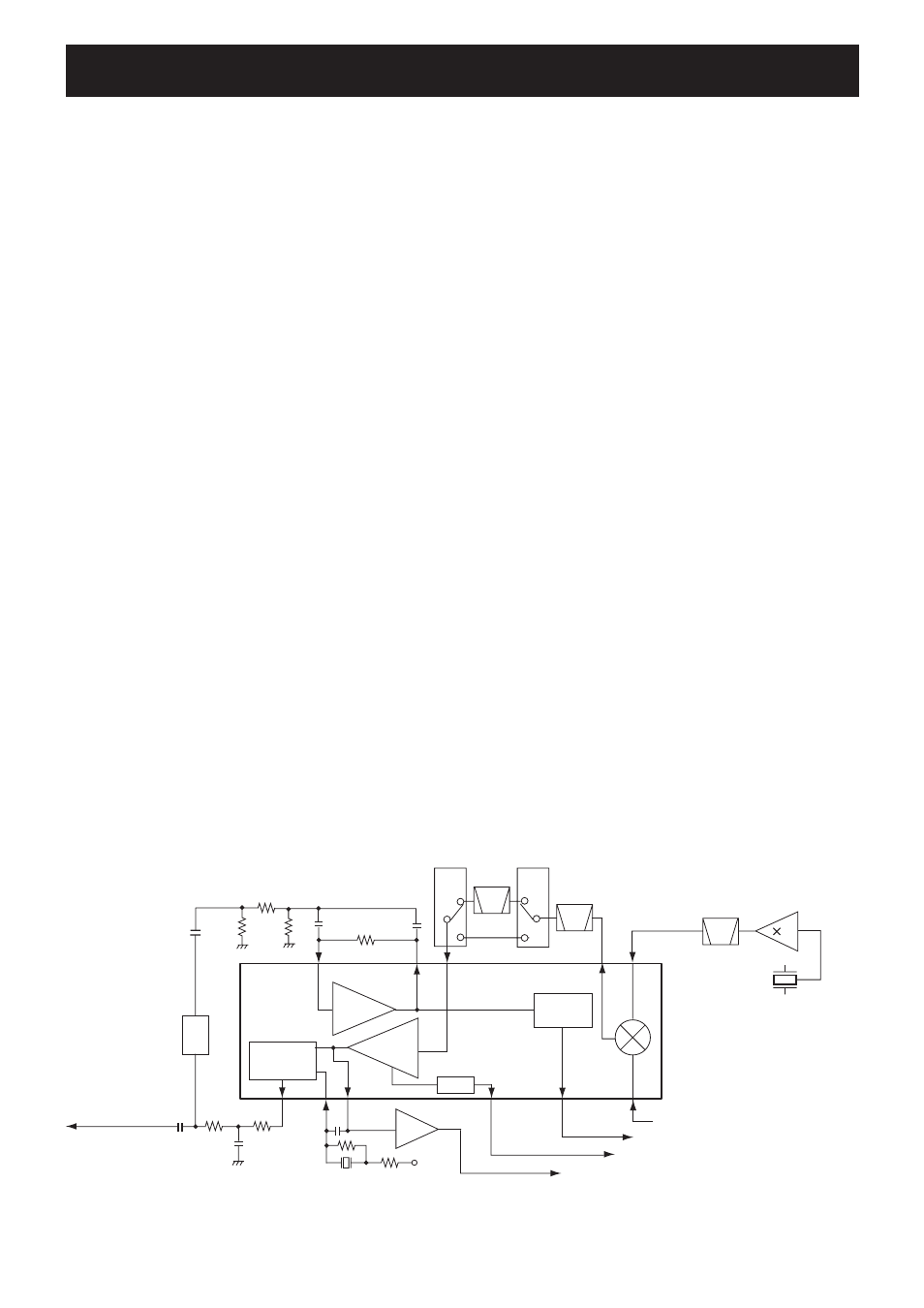
2ND IF CIRCUITS
The 1st IF signal is conver ted into the 2nd IF signal,
amplified and demodulated in the IF IC.
The 1st IF signal from the 1st IF amplifier (Q12) is applied
to the IF IC (IC5, pin 16). The applied signal is converted
into the 2nd IF signal by being mixed with the 2nd LO signal
from X1 via tripler (Q3, L3, L2, C32−C35).
The converted 2nd IF signal is output from pin 3, and
passed through the 2nd IF filter (FI1). The filtered 2nd IF
signal is passed through (bypassed) another 2nd IF filter
(FI2) via filter switches (D1 on input side; D2 on output
side). The filtered signal is then applied to the IF IC (IC5, pin
5), and amplified by 2nd IF amplifier. The amplified signal is
FM-demodulated by quadrature detector (IC5, pins 10, 11;
X3).
The demodulated AF signals are output from pin 9, then
applied to the AF circuits.
AF CIRCUITS
The demodulated AF signals from the IF IC are amplified
and fi ltered at AF circuits.
This transceiver employs the base band IC for audio signal
processing for both transmit and receive. The base band
IC is an audio processor and composed of pre-amplifier,
compressor, expander, scrambler, etc. in its package.
The demodulated AF signals from IF IC (IC5, pin 9) are
passed through Digital/Analog switch (IC8, pins 2, 15), and
applied to the base band IC (IC2, pin 23).
The applied AF signals are amplified at the amplifier section
and level adjusted at the volume controller section, then
suppressed unwanted 3 kHz and higher audio signals at
LPF. The filtered AF signals are applied (bypassed) the TX/
RX HPF, scrambler, de-emphasis sections in sequence.
The TX/RX HPF filters out 250 Hz and lower audio signals,
and the de-emphasis circuit obtains –6 dB/oct of audio
characteristics. The expander expands the compressed
audio signals and also noise reduction function is provided.
The AF signals are then level adjusted at the volume
controller section and amplified at the amplifier section, then
output from pin 20 (IC2).
D/A converter
(IC6)
Mixer
RSSI
Quadrature
detector
2
1
1st IF signal from the IF amplifier (Q12)
16
Noise
detector
+5V
X3
11
10
IF IC (IC5)
Filter
amp.
Limiter
amp.
Demodulated signals
to the AF circuits
• 2nd IF AND DEMODULATOR CIRCUITS
9
“NOIS” signal to the CPU (IC14: pin 113)
“RSSI” signal to the CPU (IC14: pin 71)
“D_IF” signal to the optional digital unit via J2
13
12
Q3
X1
15.3 MHz
45.9 MHz
BPF
2
3
Q13
Buffer
8
7
3
5
FI1
FI2
N/W
SW
N/W
SW
D2
D1
